Integrated circuit logic with self compensating block delays

a technology of integrated circuit logic and delay delay, which is applied in the field of minimizing path delay variation in integrated circuits, can solve the problems of reducing logic path variability, affecting the stability of logic paths, and not responding uniformly to all feature types, so as to reduce logic path variability

Active Publication Date: 2005-09-01
GLOBALFOUNDRIES US INC
View PDF4 Cites 108 Cited by
  • Summary
  • Abstract
  • Description
  • Claims
  • Application Information

AI Technical Summary

Benefits of technology

[0010] It is yet another purpose of the invention to reduce logic path variability.
[0011] The present invention relates to an integrated circuit (IC) including at least one combinational logic path. The combinational logic path includes two types of logic blocks cells that compensate each other for fabrication parameter effects on cell transistors. The two types may be dense cells with field effect transistor (FET) gates on contacted pitch and isolated cells with FET gates on wider than contacted pitch. Dense cell delay changes from the FET gates being printed out of focus are offset by isolated cell delay changes.

Problems solved by technology

Unfortunately, all feature types do not respond uniformly.
This dichotomy has become especially troublesome as image dimensions have shrunk.
For timing critical applications, e.g., where the clock is gating a latch at the multiplier output, the later arrival of the multiplier results and earlier arrival of the clock can cause the latch to latch wrong data.

Method used


Image

  • Integrated circuit logic with self compensating block delays
  • Integrated circuit logic with self compensating block delays
  • Integrated circuit logic with self compensating block delays

Examples


Embodiment Construction

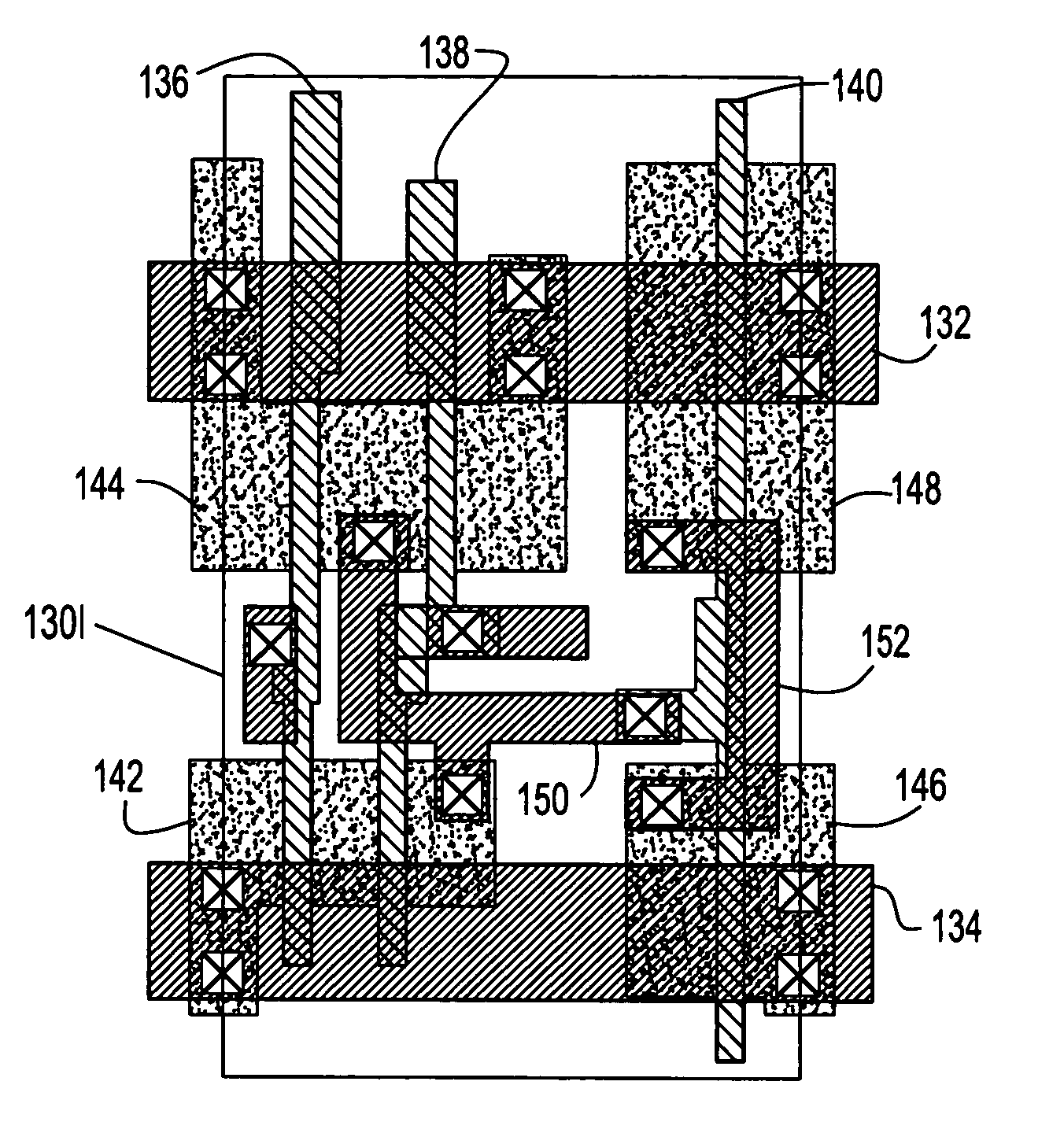
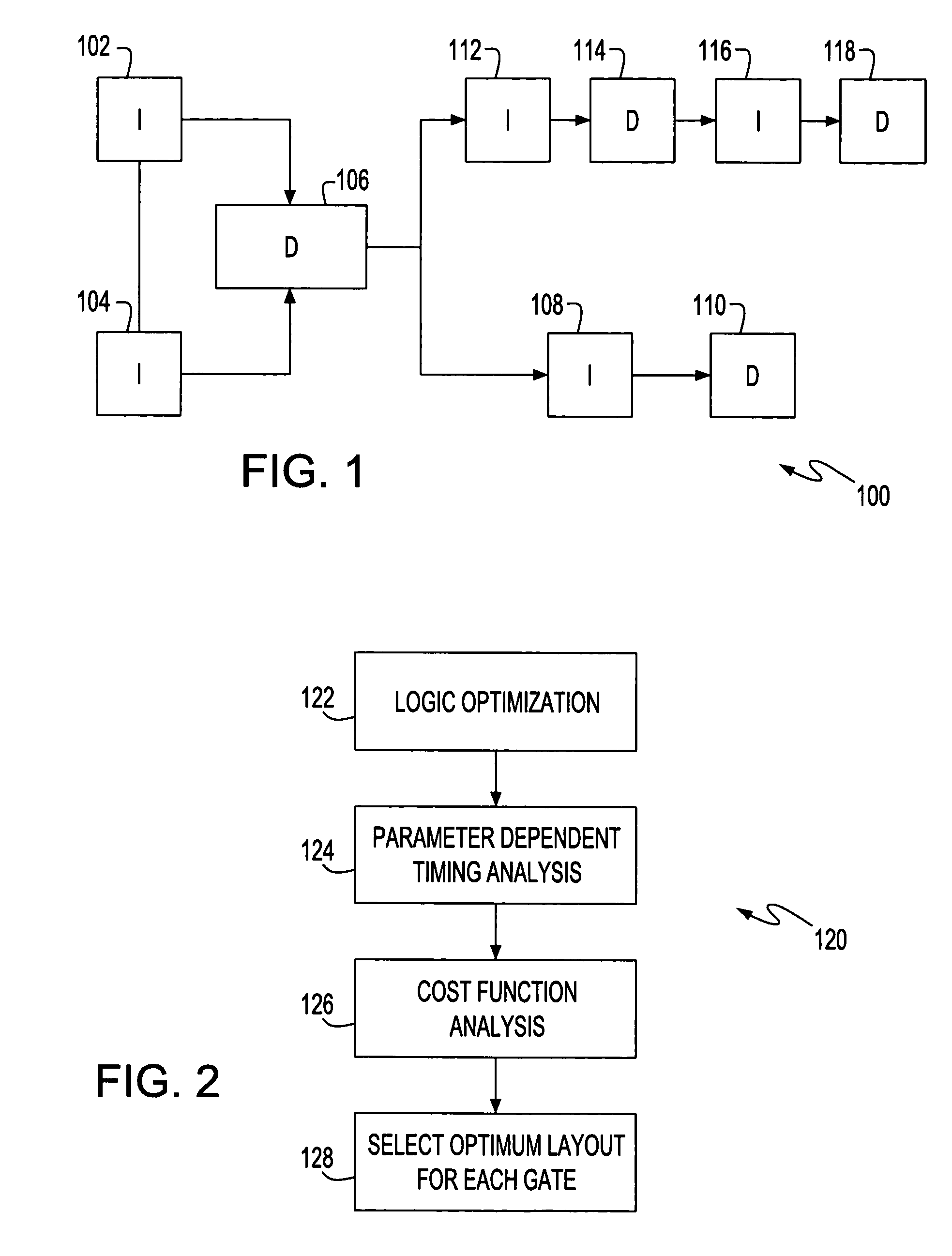
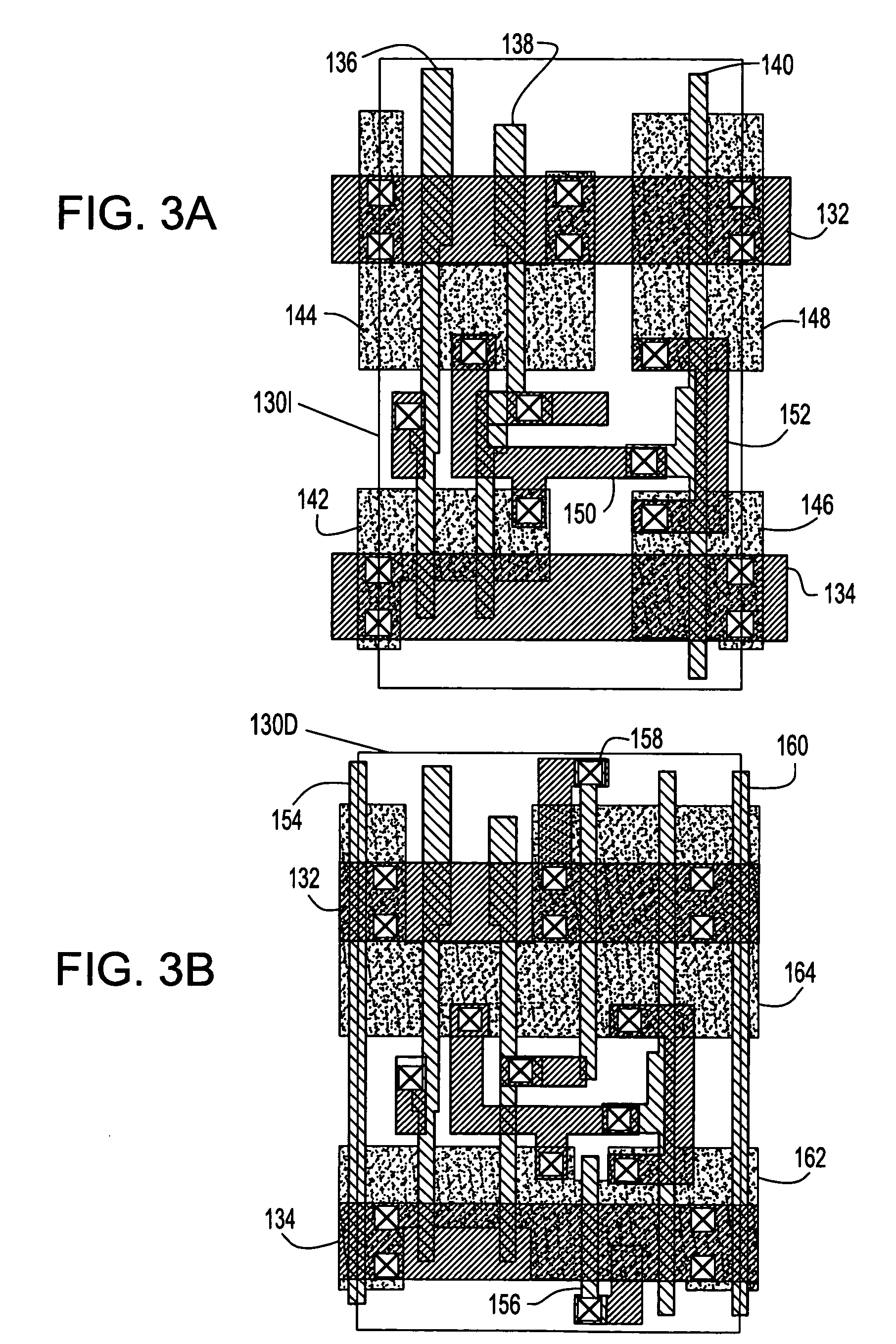
[0016] Turning now to the drawings and, more particularly, FIG. 1 shows an example of combinational logic in a cross section 100 according to a preferred embodiment of the present invention. The cross section 100, which may be on or part of an integrated circuit (IC) chip, includes logic blocks 102, 104, 106, 108, 110,112, 114, 116, 118, e.g., standard cell logic gates or macros, selected to compensate each other for individual performance deviations from nominal. In this particular example, alternating logic blocks are selected to have an opposite performance response to a particular fabrication parameter, e.g., focus variation in printing one or more mask level. So, for example, as a particular level (e.g., device or field effect transistors (FETs) gate layer) is printed on a chip site more and more out-of-focus, chip delay increases through logic blocks 102, 104, 108, 112 and 116 and decreases through logic blocks 106, 110, 114 and 118. Similarly, as the level is printed on anoth...


PUM


Abstract

An integrated circuit (IC) including at least one combinational logic path. The combinational logic path includes two types of logic blocks cells that compensate each other for fabrication parameter effects on cell transistors. The two types may be dense cells with field effect transistor (FET) gates on contacted pitch and isolated cells with FET gates on wider than contacted pitch. Dense cell delay changes from the FET gates being printed out of focus are offset by isolated cell delay changes.

Description

BACKGROUND OF THE INVENTION [0001] 1. Field of the Invention [0002] The present invention generally relates to integrated circuits and more particularly to minimizing path delay variations in integrated circuits. [0003] 2. Background Description [0004] A typical integrated circuit (IC) chip includes a stack of several levels or sequentially formed layers of shapes. Each layer is stacked or overlaid on a prior layer and patterned to form the shapes that define devices (e.g., field effect transistors (FETs)) and connect the devices into circuits. In a typical state of the art complementary insulated gate FET process, such as what is normally referred to as CMOS, layers are formed on a wafer to form the devices on a surface of the wafer. Further, the surface may be the surface of a silicon layer on a silicon on insulator (SOI) wafer. A simple FET is formed by the intersection of two shapes, a gate layer rectangle on a silicon island formed from the silicon surface layer. Each of these ...

Claims


Application Information

Patent Timeline
Patent Type & Authority Applications(United States)
IPC IPC(8): H01L27/118G06F17/50H01L21/82H01L27/02H01L27/092H01L29/00H03K5/13
CPCH01L27/092H01L27/0207
Inventor GUPTA, PUNEETHENG, FOOK-LUENKUNG, DAVID S.OSTAPKO, DANIEL L.
Owner GLOBALFOUNDRIES US INC
Why Eureka
Try Eureka