Electronic device with touching unit

Inactive Publication Date: 2005-09-08
ASUSTEK COMPUTER INC
View PDF3 Cites 0 Cited by
  • Summary
  • Abstract
  • Description
  • Claims
  • Application Information

AI Technical Summary

Benefits of technology

[0009] In view of the foregoing, the present invention is to provide an electronic device, which comprises a touching unit made by plastic lamina for reducing the height difference between the touching unit and the shell of the computer main body.
[0011] As mentioned above, the electronic device of the invention comprises a touching unit, which is integrally formed by stamping plastic materials. The thickness of the touching unit is very thin, and, therefore, the height difference between the touching unit and the shell of the computer main body can be reduced. Compared to the prior art, the height difference between the touching unit and the shell of the main body of the electronic device of the present invention is reduced, and the design of the present invention shows better integrity. In addition, since the touching unit is connected to the computer main body and faces to the detecting unit, the height difference is reduced and the dust accumulation between the touching pad frame and the touching pad as described in the prior art would not occur. Further, the touching unit produced by the stamping process is thinner and the cost of the stamping process is cheaper, so that the production cost can be reduced.

Problems solved by technology

As a result, dust may accumulate in the gap between the touch pad frame 13 and touch pad 12, and moreover, the beauty of the design for the electronic device 1 may be affected due to lack of integrity.

Method used


Image

  • Electronic device with touching unit
  • Electronic device with touching unit
  • Electronic device with touching unit

Examples


Embodiment Construction

[0017] The present invention will be apparent from the following detailed description, which proceeds with reference to the accompanying drawings, wherein the same references relate to the same elements.

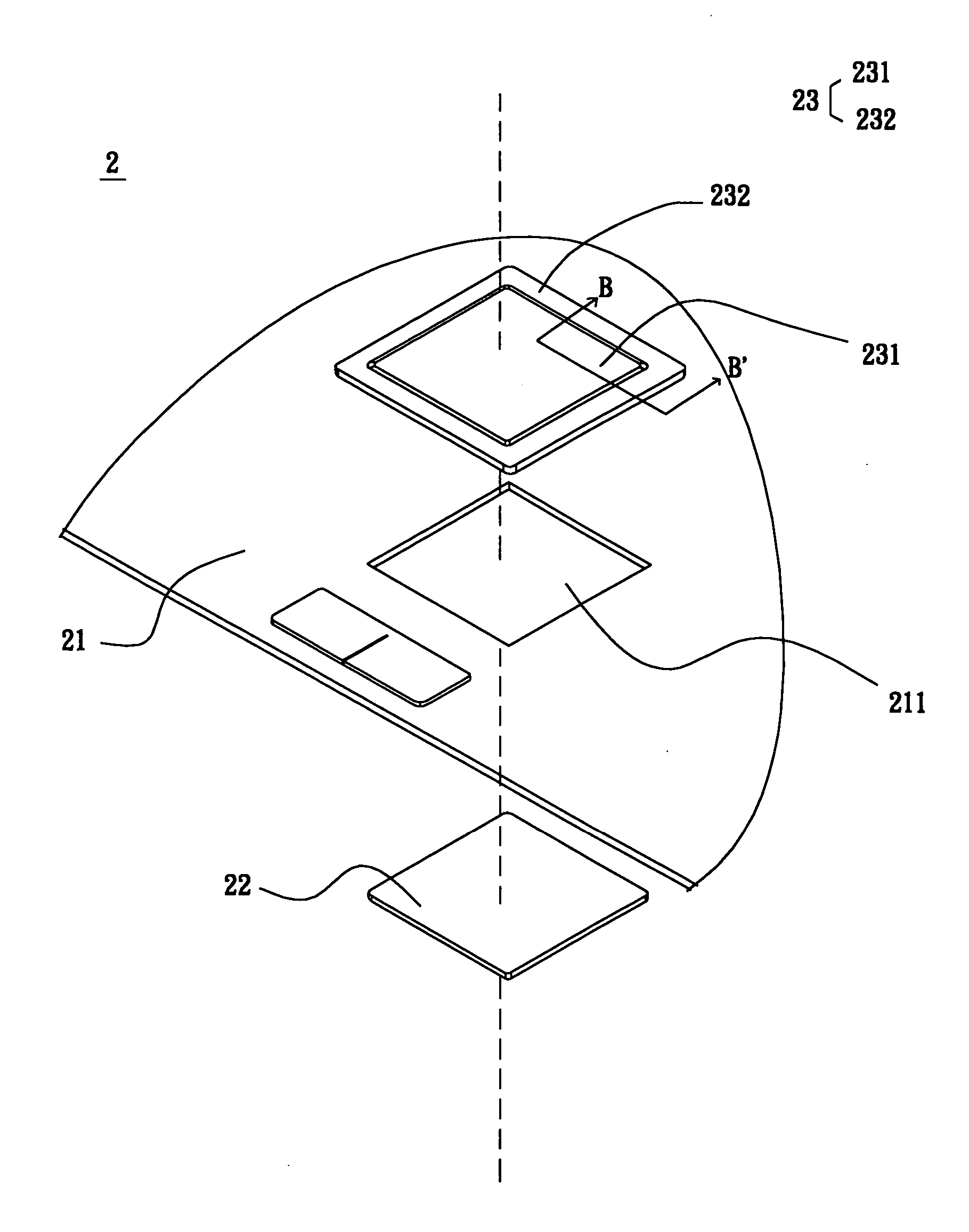
[0018] As shown in FIG. 3, the electronic device 2 according to a preferred embodiment of the invention comprises a shell 21, a detecting unit 22 and a touching unit 23.

[0019] The shell 21 is a shell of a portable data processor, such as a shell of a notebook computer main body. The shell 21 has at least one opening 211.

[0020] The detecting unit 22 is disposed in the shell and below the opening 211. The detecting unit 22 is a touch pad, and plural sensing circuits are distributed on the surface thereof. When an object (for example, a finger or a stylus pen) moves on the touch pad, a signal for controlling the movement of a cursor is produced due to a change in the capacitance or the resistance of the sensing circuit.

[0021] The touching unit 23 has a first portion 231 (the gray pa...


PUM


Abstract

An electronic device includes a shell, a detecting unit and a touching unit. In this case, the shell has at least one opening. The detecting unit is disposed in the shell and below the opening. The touching unit has a first portion and a second portion. The touching unit covers the opening. The first portion faces to the detecting unit. The second portion is disposed around the first portion and is connected to the shell.

Description

BACKGROUND OF THE INVENTION [0001] 1. Field of Invention [0002] The invention relates to an electronic device and, in particular, to an electronic device comprising a touching unit made by plastic lamina, whereby the height difference between the touching unit and the shell of the computer main body can be reduced. [0003] 2. Related Art [0004] As technology improves, many devices for generating control signals have been invented in recent years in the field of portable electronic products, so that the cursor can be moved on the display screen according to the control signals. These devices, for example, include mice, track balls, joysticks, touch pads, track points, and etc. [0005] Among those devices, the touch pad is an invention that brings a lot of convenience. It not only allows the user to control the cursor on the screen by moving his / her finger thereon in coordination with clicking the touching pad buttons, but also possesses a function similar to that of the left and right ...

Claims


Application Information

Patent Timeline
IPC IPC(8): G09G5/00
CPCG06F1/1613G06F3/03547G06F3/00G06F1/169
Inventor HO, MING YUAN
Owner ASUSTEK COMPUTER INC
Why Eureka
Try Eureka