Semiconductor device

Active Publication Date: 2017-09-07
MITSUBISHI ELECTRIC CORP
View PDF0 Cites 5 Cited by
  • Summary
  • Abstract
  • Description
  • Claims
  • Application Information

AI Technical Summary

Benefits of technology

[0005]In view of the above-described problem, an object of the present inven

Problems solved by technology

However, a fine pattern cannot be formed because the film thicknesses of electrodes are large.
Even if a fine pattern having a large difference in height and a high aspect ratio can be formed, an electrode fall-down or a crack in a protective film at an electrode step portion is caused by stress from an external package, resulting in a reduction in reliability.
On the othe

Method used


Image

  • Semiconductor device
  • Semiconductor device

Examples


first embodiment

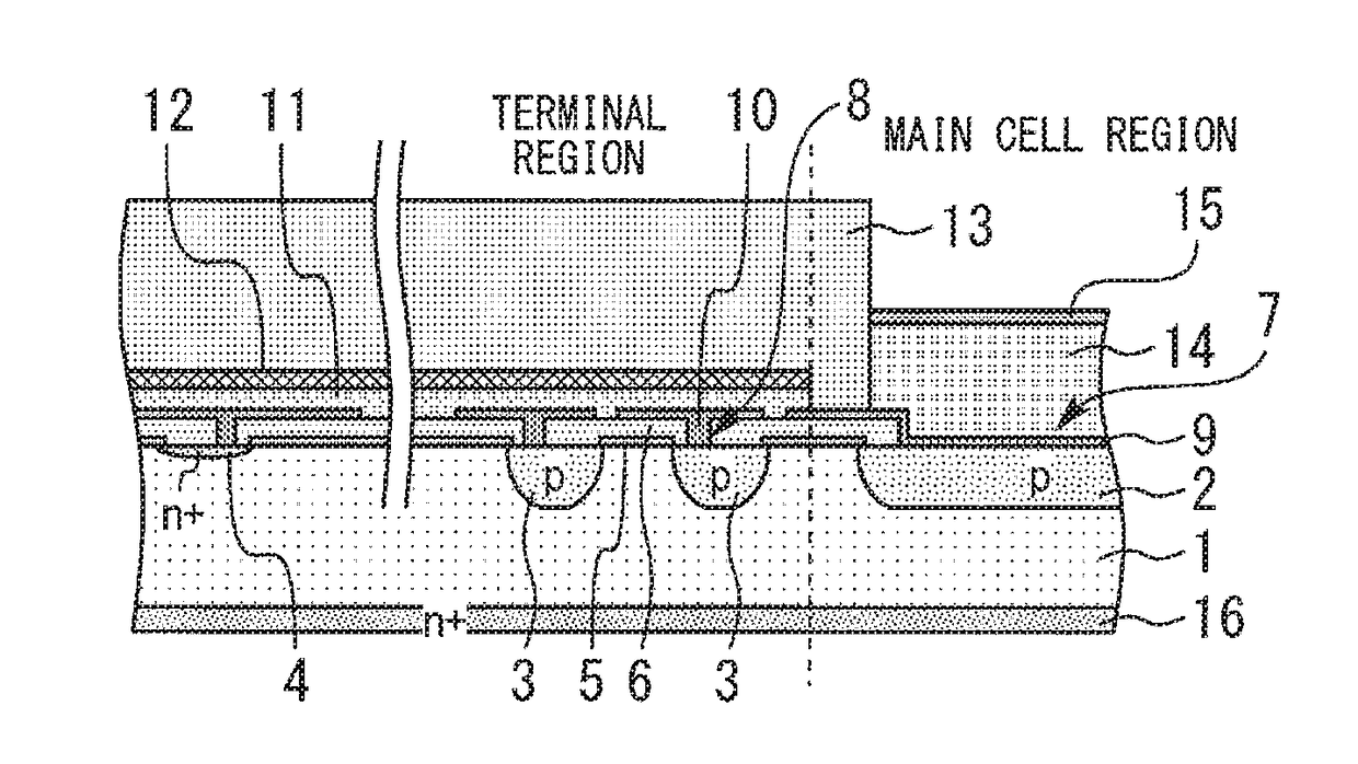
[0013]FIG. 1 is a sectional view of a semiconductor device according to a first embodiment of the present invention. In a main cell region, a p-type anode region 2 is formed in a major surface of a Si substrate 1. In a terminal region outside the main cell region, a plurality of p-type ring regions 3 and an Ni+-type ring region 4 are formed in the major surface of the Si substrate 1. An SiO2 oxide film 5 and a TEOS oxide film 6 are formed on the major surface of the Si substrate 1. The SiO2 oxide film 5 and the TEOS oxide film 6 have first and second contact holes 7 and 8 formed on the p-type anode region 2 and the p-type ring regions 3, respectively.

[0014]An AlSi electrode 9 is formed in the first contact hole 7 and connected to the p-type anode region 2. A plurality of AlSi electrodes 10 are respectively formed in the plurality of second contact holes 8 and respectively connected to the plurality of p-type ring regions 3. An SiN semi-insulating film 11 and an SiN insulating film 1...

second embodiment

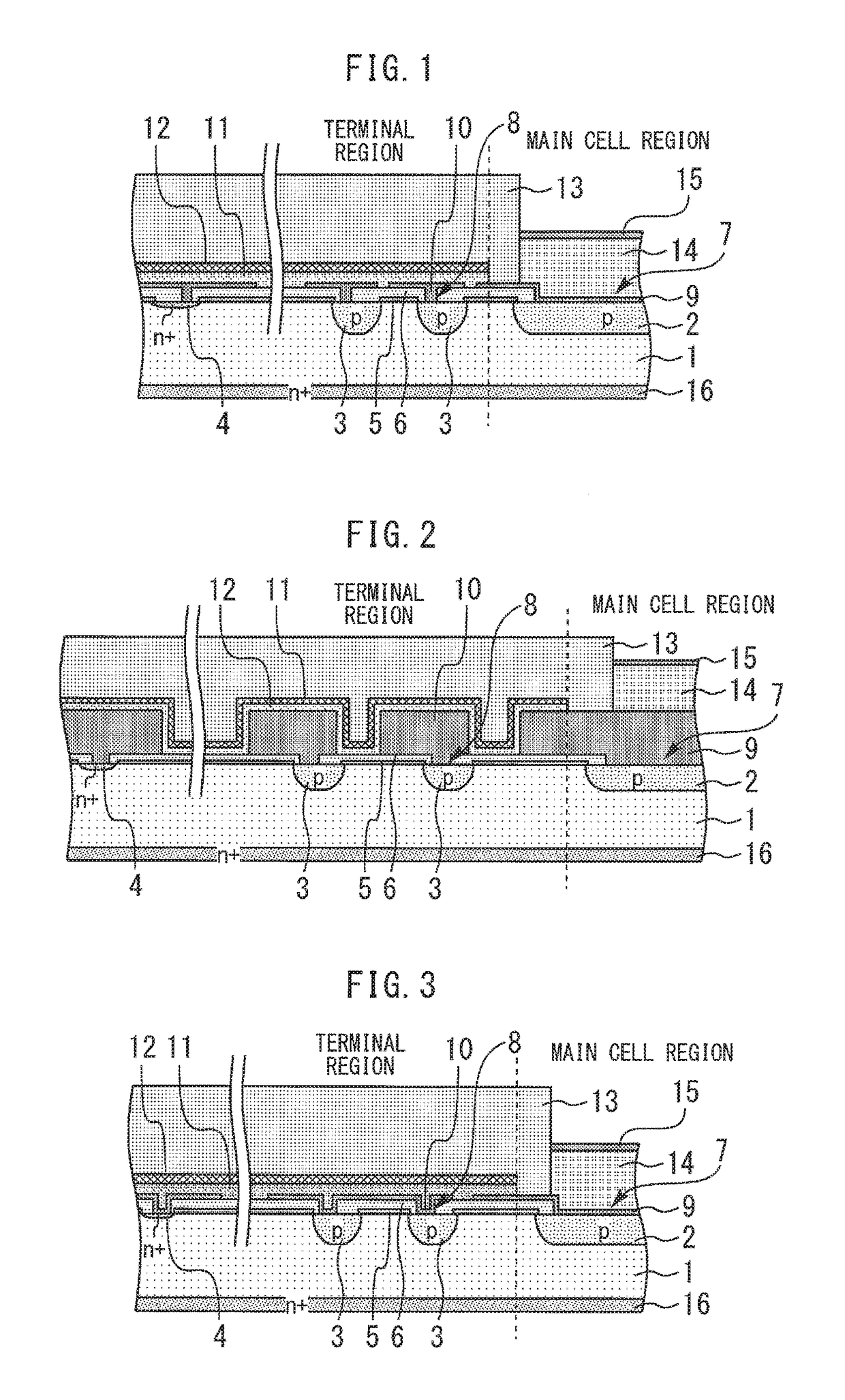
[0023]FIG. 3 is a sectional view of a semiconductor device according to a second embodiment of the present invention. The second embodiment differs from the first embodiment in that the AlSi electrodes 10 do not completely fill the second contact holes 8 but the SiN semi-insulating film 11 completely fills the second contact holes 8. Filling with the SiN semi-insulating film 11 in this way produces an equipotential condition even when a disconnection occurs as a result of degradation of contact coverage in the terminal region. The potential at the time of reverse biasing can therefore be borne dividedly by the FLRs and the FPs so that the withstand voltage is stabilized. In other respects, the construction and advantageous effects of the present embodiment are the same as those of the first embodiment.

[0024]In the first and second embodiments, barrier metal such as TiN or TiW may he formed under the AlSi electrodes 9 and 10. Damage at the time of forming of the electrodes to which e...


PUM


Abstract

A semiconductor device includes; a semiconductor substrate including a major surface; a first diffusion region in the major surface in a main cell region; a second diffusion region in the major surface in a terminal region; an insulating film on the major surface and having first and second contact holes on the first and second diffusion regions respectively; a first electrode in the first contact hole and connected to the first diffusion region; a second electrode in the second contact hole and connected to the second diffusion region; a semi-insulating film covering the second electrode; and a third electrode on the first electrode, wherein the first and second electrodes are made of the same material, the first electrode does not completely fill the first contact hole, the second electrode completely fills the second contact hole, and the third electrode completely fills the first contact hole.

Description

BACKGROUND OF THE INVENTIONField[0001]The present invention relates to a semiconductor device including a diode structure for a power semiconductor.Background[0002]In a diode for a power semiconductor, a contact hole in a main cell region is filled with a thick AlSi electrode in order to cause a large current to flow vertically. Also, a field limiting ring (FLR) structure is adopted as a terminal structure, and field plate (FP) electrodes are formed on a guard ring (GR) and field limiting rings (FLRs), thereby enabling a depletion layer to extend easily (see, for example, JP 09-023016 A). Further, a semi-insulating protective film is formed on the entire surface of the terminal region for the purpose of stabilizing the potential.[0003]In recent years, there has been a trend to replace wire bonding (WB) with direct lead bonding (DLB) as a method of joining a region for causing a current to flow through a main cell region. Therefore, there have been increasing cases where an electrode...

Claims


Application Information

Patent Timeline
IPC IPC(8): H01L23/00H01L29/40H01L29/66H01L29/868H01L21/761H01L29/06H01L29/45
CPCH01L23/562H01L29/0623H01L29/402H01L29/408H01L29/6609H01L29/868H01L21/761H01L29/401H01L29/45H01L29/40H01L29/861H01L23/3157H01L29/404H01L29/66128H01L29/8611H01L29/0638H01L29/1602H01L29/1608H01L29/2003H01L29/0619
Inventor FUJII, HIDENORI
Owner MITSUBISHI ELECTRIC CORP
Why Eureka
Try Eureka