Method for mapping logic design memory into physical memory devices of a programmable logic device

a logic design and memory technology, applied in the field of implementing logic design memory in physical memory devices of a programmable logic device, can solve the problems of not taking into account the possibility, the technique of implementing logic design memory into physical memory devices is limited, and it is impossible to attempt to lay out logic without such softwar

Inactive Publication Date: 2005-09-15
ALTERA CORP
View PDF8 Cites 29 Cited by
  • Summary
  • Abstract
  • Description
  • Claims
  • Application Information

AI Technical Summary

Problems solved by technology

With current larger devices, it would be impractical to attempt to lay out the logic without such software.
Known techniques for implementing logic design memory into physical memory devices are limited with respect to several aspects.
Known techniques do not take into account the possibility of having more than one type of physical memory device in a single programmable logic device.
Another shortcoming of known techniques for implementing logic design memory in physical memory devices is the inability to guarantee that all location constraints will be met and the inability to prevent problems from arising due to conflicting constraints.
Yet another shortcoming of the known techniques is that typically the resultant physical devices are not optimized for efficiency in terms of resource usage, timing constraints, power demand, as well as other factors.

Method used


Image

  • Method for mapping logic design memory into physical memory devices of a programmable logic device
  • Method for mapping logic design memory into physical memory devices of a programmable logic device
  • Method for mapping logic design memory into physical memory devices of a programmable logic device

Examples


Embodiment Construction

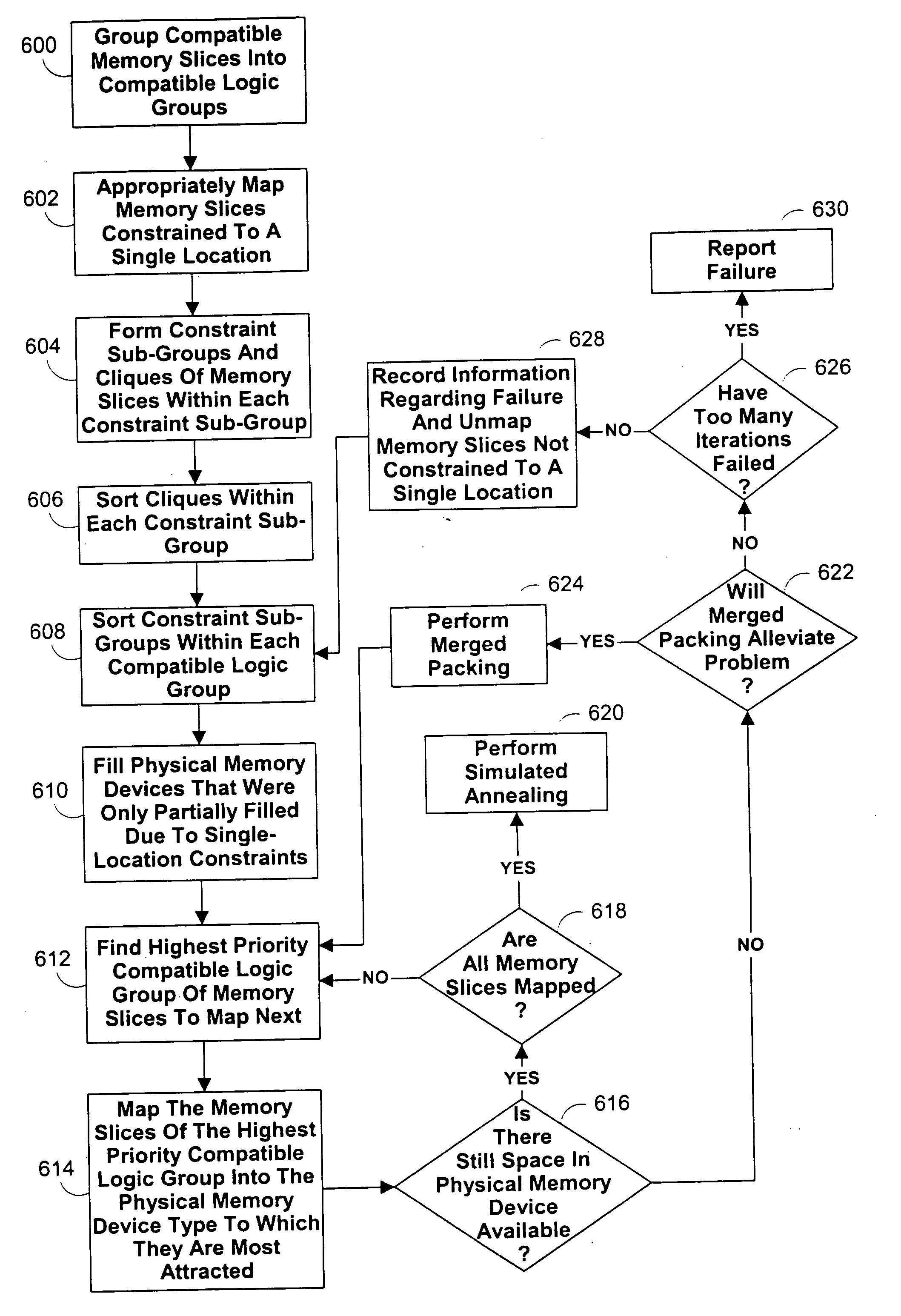
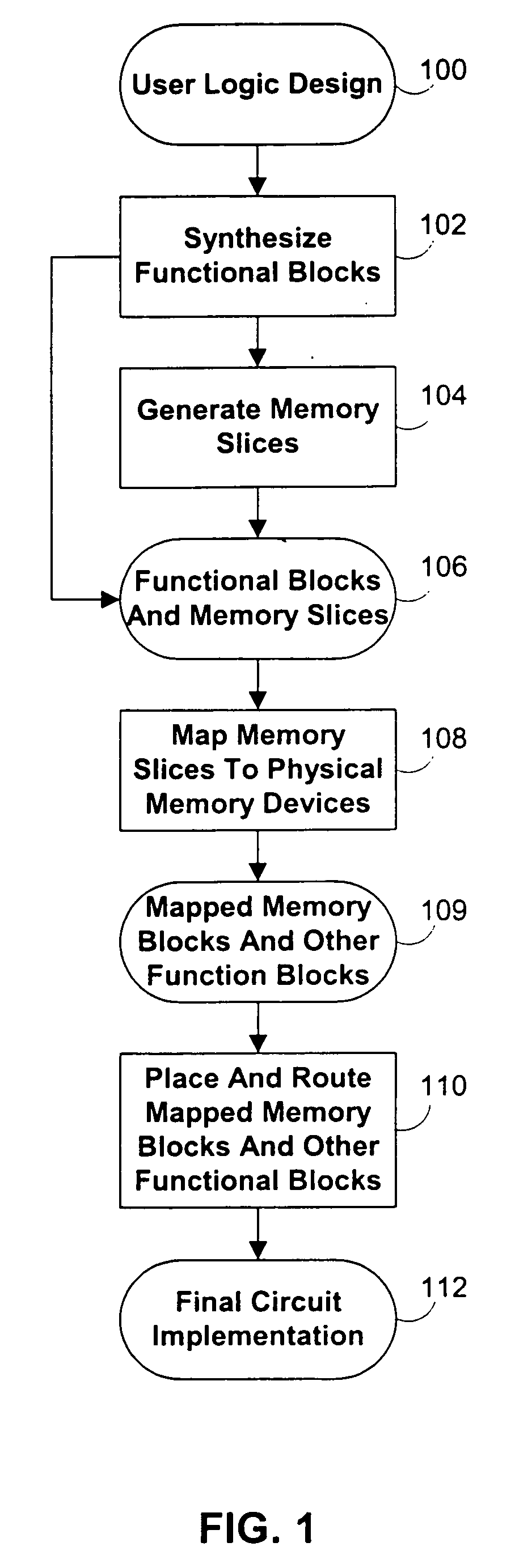
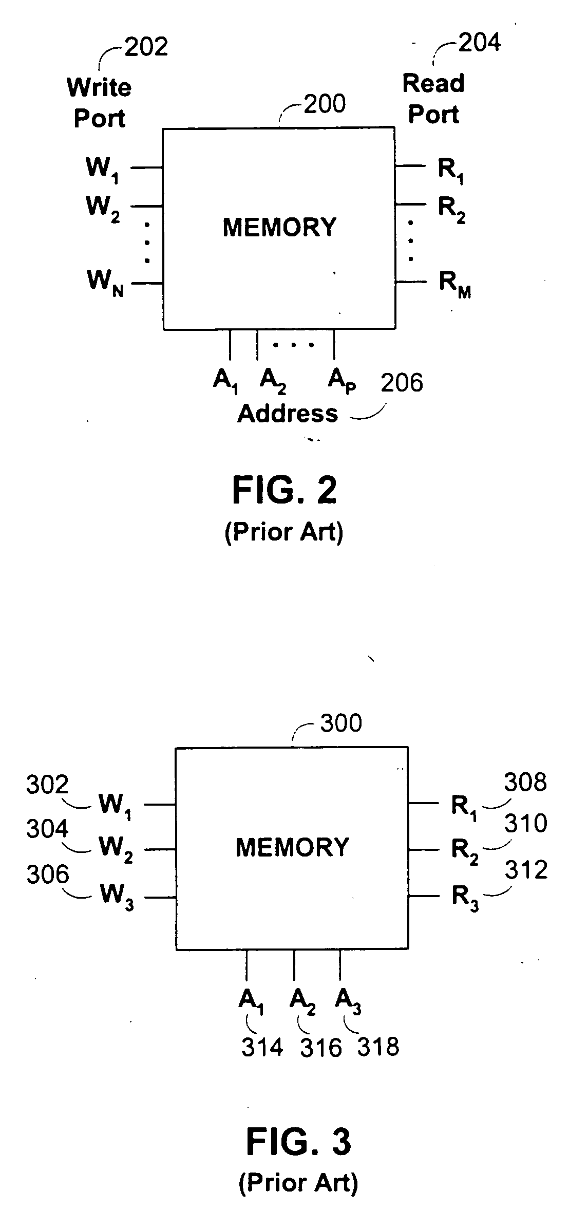
[0038] The present invention maps logic design memory (as defined by a user-created logic design) into physical memory devices located on a programmable logic device. Logic design memory may include any suitable form of memory that may be used in a user logic design, such as any suitable type of random access memory. Physical memory devices may include any suitable memory device that may be used to implement logic design memory, such as any form of physical random access memory, EPROM, logic array blocks implemented as memory devices, or any other suitable physical element or elements of a programmable logic device. The physical memory devices of a programmable logic device may vary according to any suitable specification, such as capacity, speed, structure, size, or any other suitable specification.

[0039] The present invention is primarily described herein in terms of a logic design to hardware application. The logic design to hardware application may be any suitable software, har...


PUM


Abstract

A method is provided for mapping logic design memory into physical memory devices of a programmable logic device. User constraints and physical constraints may be taken into account in generating the mapping solution. Functional block layout on the programmable logic device may be taken into account when generating the mapping solution. Multiple types of physical memory types may be considered and logic design memory may be mapped to those types of physical memory devices that are determined to be the most appropriate. A mapping solution may be optimized using, for example, simulated annealing.

Description

[0001] This application is a continuation of co-pending U.S. patent application Ser. No. 10 / 294,836, filed on Nov. 14, 2002, which is hereby incorporated by reference herein in its entirety.BACKGROUND OF THE INVENTION [0002] The present invention relates to implementing a user logic design in a programmable logic device, and more particularly, the present invention relates to implementing logic design memory in physical memory devices of a programmable logic device. [0003] Programmable logic devices are well known. Early programmable logic devices were one-time configurable. For example, configuration may have been achieved by “blowing” (i.e., opening) fusible links. Alternatively, the configuration may have been stored in a programmable read-only memory. Those devices generally provided the user with the ability to configure the devices for “sum-of-products” (or “P-TERM”) logic operations. Later, such programmable logic devices incorporating erasable programmable read-only memory (...

Claims


Application Information

Patent Timeline
Patent Type & Authority Applications(United States)
IPC IPC(8): G06F17/50
CPCG06F17/5054G06F30/34
Inventor FUNG, RYANPADALIA, KETAN
Owner ALTERA CORP
Why Eureka
Try Eureka