Multiple layers of memory implemented as different memory technology

a memory technology and memory layer technology, applied in the field of data storage and computer memory, can solve the problems of increasing the size of the die, consuming relatively large amounts of surface area (e.g., silicon die area), and large volume of the conventional sram cell

Inactive Publication Date: 2010-08-05
UNITY SEMICON
View PDF19 Cites 27 Cited by
  • Summary
  • Abstract
  • Description
  • Claims
  • Application Information

AI Technical Summary

Problems solved by technology

A drawback to implementing SRAM 101 in multiprocessor 120 is that conventional SRAM cells are relatively large (e.g., compared to DRAM cells), and, thus, consume relatively large amounts of surface area (e.g., silicon die area).
A usual drawback to embedding DRAM and FLASH memory technologies in the same substrate that contains the multiple processors is that they increase the die size, which, in turn, leads to hig

Method used


Image

  • Multiple layers of memory implemented as different memory technology
  • Multiple layers of memory implemented as different memory technology
  • Multiple layers of memory implemented as different memory technology

Examples


Embodiment Construction

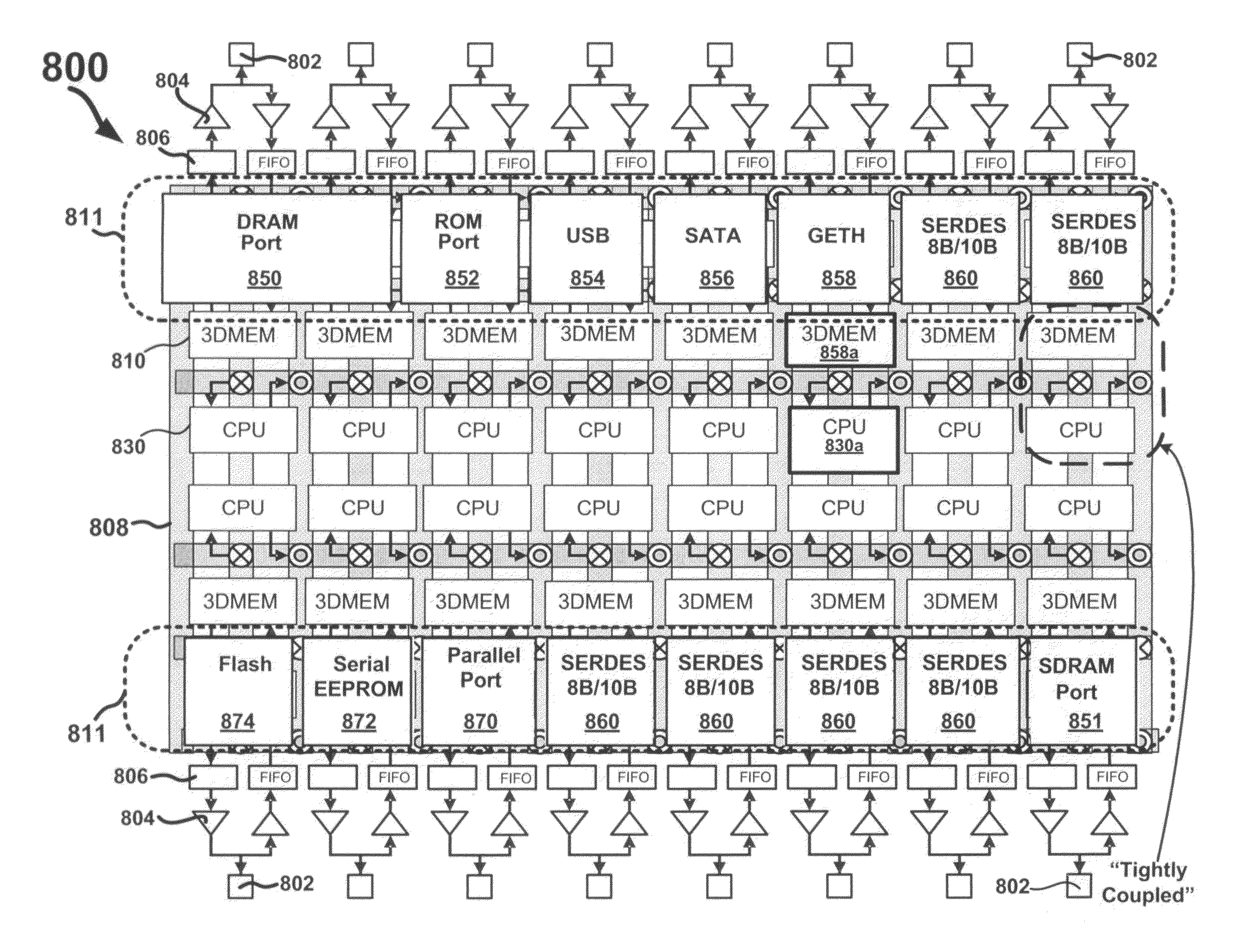
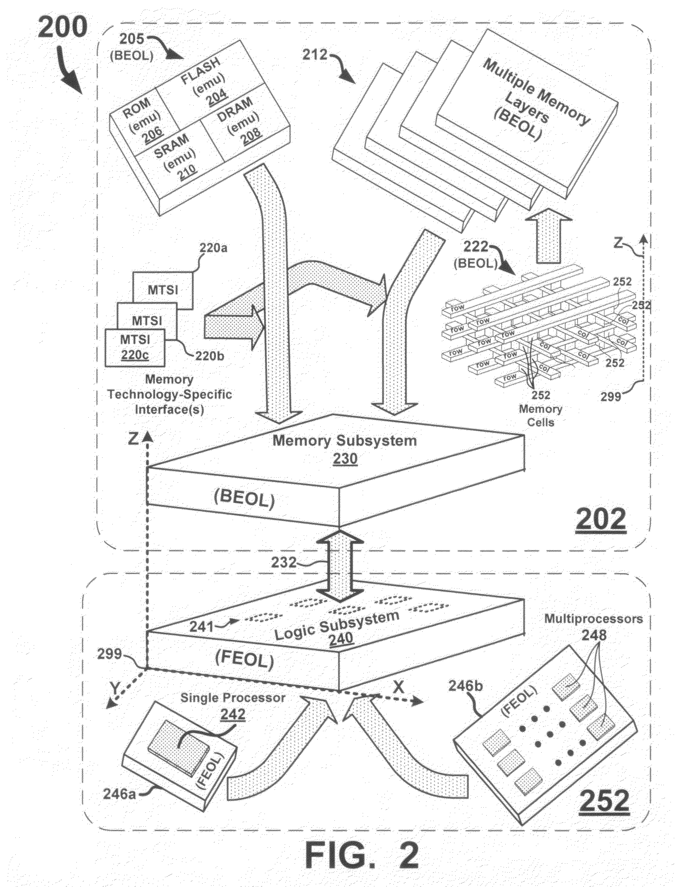
[0015]FIG. 2 depicts an exploded diagram of a processor-memory system 200 in accordance with at least one embodiment of the invention. As shown, processor-memory system 200 includes a memory portion 202 and a logic portion 252 as memory subsystem 230 and logic subsystem 240, respectively, both being communicatively coupled via, for example, trans-layer interconnections 232 operative to electrically couple the logic portion 252 with the memory portion 202. Logic subsystem 240 includes logic configured to at least access memory subsystem 230 to perform data operations (e.g., write or read data). In some cases, logic subsystem 240 can include multiple processors (“multiprocessors”) 248 formed on a substrate 246b, whereas logic subsystem 240 can include a single processor 242 formed on substrate 246a in other cases. Alternatively, logic subsystem 240 can include only a silicon wafer (e.g., fabricated FEOL) upon which memory subsystem 230 is formed directly on top of (e.g., BEOL). Regard...


PUM

PropertyMeasurementUnit
Electrical conductivityaaaaaaaaaa
Dimensionaaaaaaaaaa
Volatilityaaaaaaaaaa

Abstract

Circuits and methods that use third dimension memory as a different memory technology are described. The third dimension memory can be used for application specific data storage and/or to emulate conventional memory types such as DRAM, FLASH, SRAM, and ROM or new memory types as they become available. A processor-memory system implements a memory operable as different memory technologies. The processor-memory system includes a logic subsystem and a memory subsystem, which includes third dimension memory cells. The logic subsystem implements memory technology-specific signals to interact with the third dimension memory cells as memory cells of a different memory technology. As such, the memory subsystem can emulate different memory technologies. The logic subsystem can be fabricated FEOL on a substrate and the memory subsystem can be fabricated BEOL directly on top of the substrate. An interlayer interconnect structure can electrically couple the logic subsystem with the memory subsystem.

Description

FIELD OF THE INVENTION[0001]Embodiments of the invention relate generally to data storage and computer memory, and more particularly, to systems, devices, and methods using multiple layers of memory as a different memory technology.BACKGROUND OF THE INVENTION[0002]Conventional semiconductor fabrication processes have reduced device geometries in the x, y and z dimensions so as to facilitate the fabrication of relatively dense, complex circuits as a “system on a chip,” or SoC. An example of a SoC is the “multiprocessor” chip, which is composed of multiple processors, various memory technologies for satisfying different data storage requirements, and specialized circuits, all of which are fabricated as an integrated circuit. One type of specialized circuit is a communications port circuit, such as a conventional universal serial bus (“USB”) port circuit. FIG. 1 depicts a functional diagram of a conventional processor-memory system 100 based on a multiprocessor 120 and various memory t...

Claims


Application Information

Patent Timeline
IPC IPC(8): G11C5/02G06F9/455G11C7/00H05K3/30
CPCG11C5/02Y10T29/4913G11C5/04
Inventor NORMAN, ROBERT
Owner UNITY SEMICON
Why Eureka
Try Eureka