Device for generating a bit line selection signal of a memory device

a memory device and bit line selection technology, which is applied in the direction of logic circuits, digital storage, instruments, etc., can solve the problems of increasing the difficulty of meeting the speed related parameters, increasing the rc delay, and increasing the specification margin, so as to improve the signal transmission speed of data and the specification margin is sufficient

Active Publication Date: 2005-09-22
INTELLECTUAL DISCOVERY CO LTD
View PDF7 Cites 0 Cited by
  • Summary
  • Abstract
  • Description
  • Claims
  • Application Information

AI Technical Summary

Benefits of technology

[0013] Against this backdrop, the present invention has been developed. The present invention provides, inter alia, a circuit for securing a sufficient specification margin required for high-speed operations in any semiconductor memory device. The present invention improves signal transmission speed of data from a bit line selected by a column address.
[0017] After the predetermined time, the voltage of the second signal outputted at the inverter chain output terminal is held at a higher voltage than the voltage of the first signal to improve the current driving capacity of the column transistor that increases the transmission speed of the signal transmitted from the bit line to the local input / output line.

Problems solved by technology

However, as the memory device is becoming highly integrated, meeting every specification of the speed related parameters is becoming increasingly more difficult.
For example, the signal lines in a highly integrated memory device are likely to be elongated more thinly, and this tends to cause more RC delays, making more difficult to meet the the speed related parameters.
However, technical problems lie in the next-generation semiconductor memory devices, such as DDR2 SDRAM, in which the external power voltage VEXT utilized is below 2.5 V, and more typically less than 1.8 V. Thus, the voltage level of Yi signal in the next generation memory devices applied to the gates of the column transistors would be lower than 1.8 V and cause very poor tAA when it is compared to the tAA of DDR SDRAM.

Method used


Image

  • Device for generating a bit line selection signal of a memory device
  • Device for generating a bit line selection signal of a memory device
  • Device for generating a bit line selection signal of a memory device

Examples


Embodiment Construction

[0026] Wherever appropriate, same reference numerals are used to refer to the same or like parts in the description and / or the drawings.

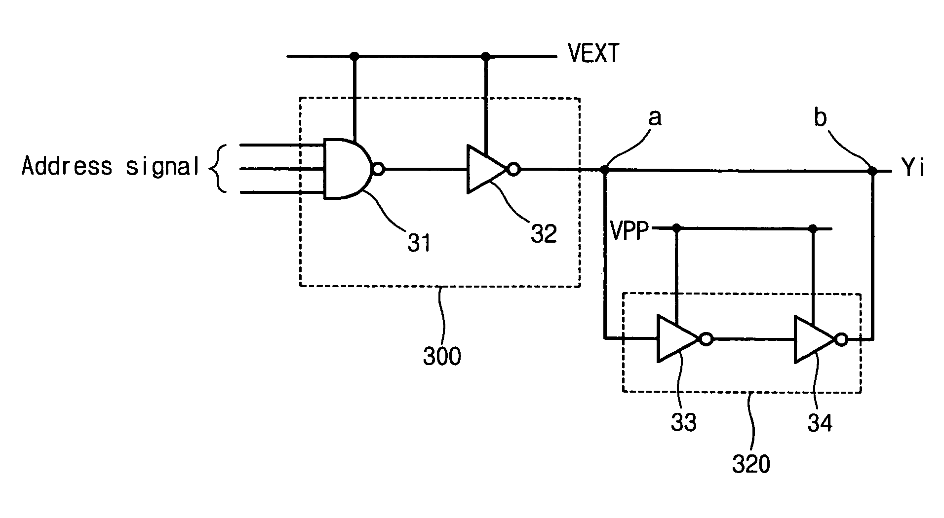
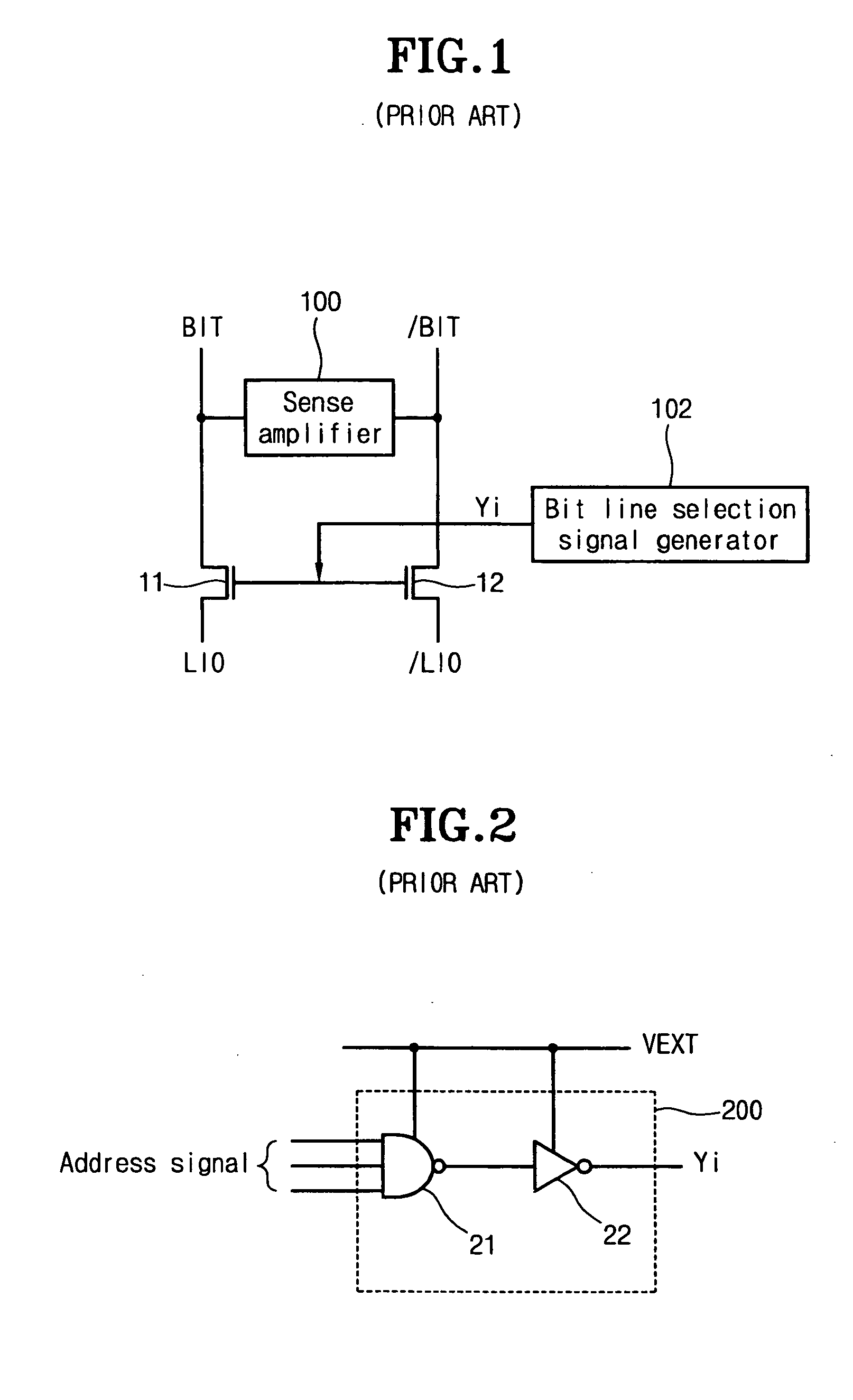
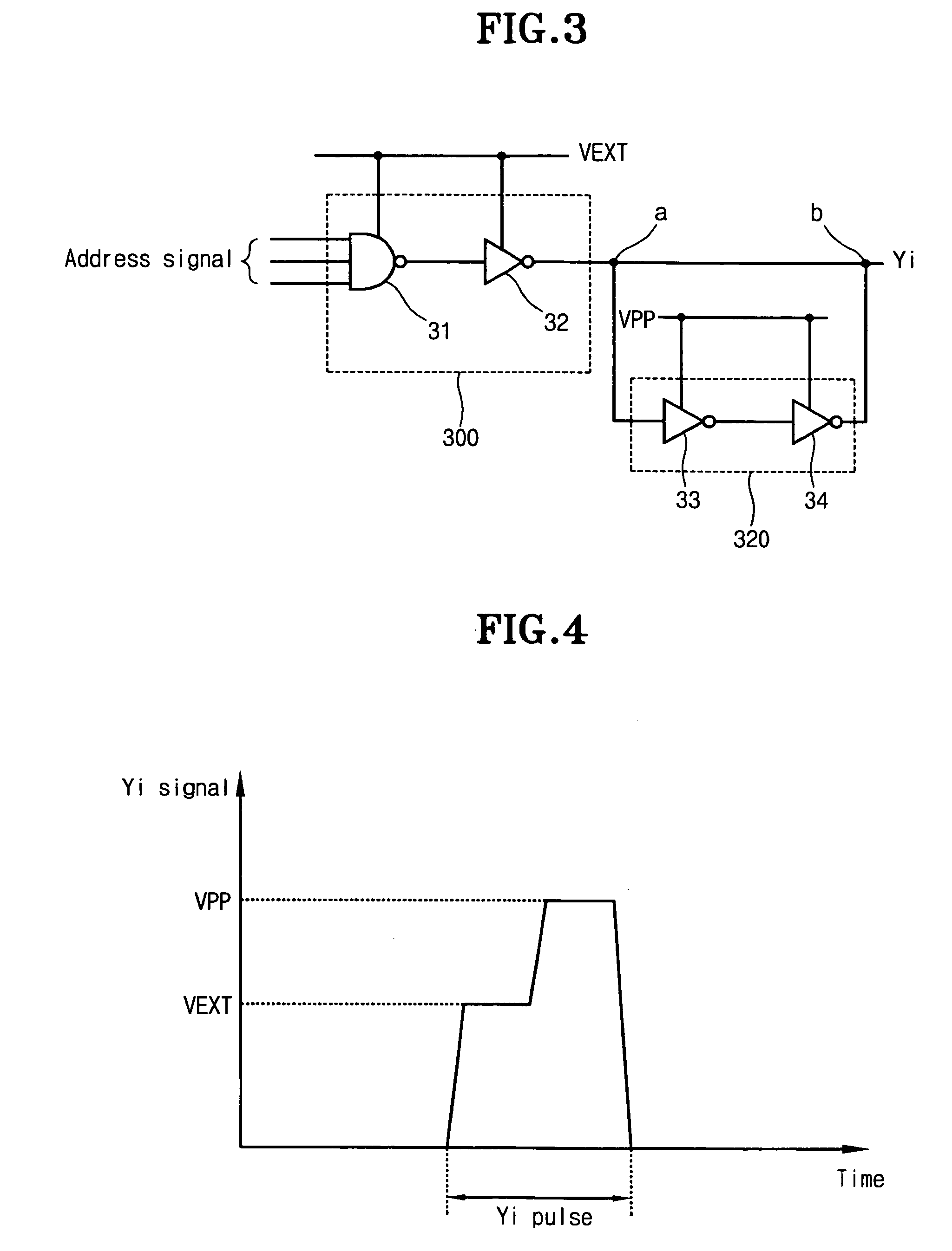
[0027] In general, a semiconductor memory device outputs data after an active command (such as a read command) is issued to enable a word line. To do so, the memory device outputs the data available on a specific bit line corresponding to the selected column address. Typically, the column address is inputted at the same time when a read command is issued. The data, which has been made available on the bit line selected by the column address, is transmitted to a data output pad through local and global lines.

[0028] It is desired to optimize the speed parameter tAA in any semiconductor memory devices, especially in those that are highly integrated. The present invention provides solutions to these technical challenges. In general, the circuit according to an embodiment of the present invention reduces the tAA by enhancing the operational performance...


PUM


Abstract

The device for generating the bit line signal to enable a column transistor that is connected to a bit line and a local line in a semiconductor memory device includes at least a column decoder and a chain of connected inverters. The column decoder decodes a column address signal. The chain of connected inverters has an input terminal for receiving a first signal outputted from the column decoder and an output terminal for outputting a second signal to drive the column transistor. The second signal voltage is held substantially same as the first signal voltage for a predetermined time. After the predetermined time, the second signal voltage is held at a higher voltage than the first signal voltage to improve the current driving capacity of the column transistor. This increases the transmission speed of the signal transmitted from the bit line to the local input / output line.

Description

BACKGROUND OF THE INVENTION [0001] 1. Field of the Invention [0002] The present invention relates generally to a device for generating a bit line selection signal in a semiconductor memory device, and more particularly to a device for generating a bit line selection signal to optimally facilitate the high speed operations of a semiconductor memory device. [0003] 2. Description of the Related Art [0004] High-speed and high-integration are the two key technological factors in the modern semiconductor memory design. However, as the memory device is becoming highly integrated, meeting every specification of the speed related parameters is becoming increasingly more difficult. For example, the signal lines in a highly integrated memory device are likely to be elongated more thinly, and this tends to cause more RC delays, making more difficult to meet the the speed related parameters. [0005] Another factor that should not be neglected to meet the speed related parameters in a memory devic...

Claims


Application Information

Patent Timeline
Patent Type & Authority Applications(United States)
IPC IPC(8): G11C11/407G11C7/10G11C7/12G11C11/408G11C11/4094G11C11/4096H03K19/013H03K19/017H03K19/082
CPCG11C7/1048G11C11/4087H03K19/01721G11C2207/002H03K19/0136G11C11/4096A47J27/002A47J36/06
Inventor KIM, YOUNG SOO
Owner INTELLECTUAL DISCOVERY CO LTD
Why Eureka
Try Eureka