
Copper alloy material for parts of electronic and electric machinery and tools

a technology of electronic and electric machinery and parts, applied in the direction of coupling contact members, transportation and packaging, contacts, etc., can solve the problems of inability to use for a long period of time, inability to improve the bending property while maintaining mechanical strength and elasticity, and inability to meet the requirements of the current generation

Inactive Publication Date: 2005-09-22
USAMI TAKAYUKI +1
View PDF20 Cites 5 Cited by
  • Summary
  • Abstract
  • Description
  • Claims
  • Application Information

AI Technical Summary

Benefits of technology

The alloy exhibits improved bending properties, stress relaxation, and plating compatibility, maintaining mechanical strength and conductivity while preventing peeling and ensuring reliable plating, thus addressing the requirements for miniaturized and high-performance electronic components.

Problems solved by technology

While inexpensive Cu—Zn alloys have been used frequently, for example, in automobiles, the Cu—Zn alloys as well as Cu—Fe alloys and Cu—Sn alloys have been unable to currently cope with the requirements for the automobile, since recent trends urgently require the terminals and connectors to be small size, and they are mostly used under severe conditions (high temperature and corrosive environment) in an engine room and the like.
The materials are also required to be excellent in stress relaxation property, and the conventional Cu—Ni—Si alloys cannot be used for a long period of time, due to increased stress load on the material and high temperatures in the working environments.
Although improvements of bending property have been investigated in ways, it has been difficult to improve the bending property while maintaining the mechanical strength and elasticity.
When unevenness (roughness) of the material surface is larger than the thickness of the plating layer, the plating is repelled from convex portions without being plated to make it impossible to uniformly plate.
While Au is generally plated on the Ni underlayer plating in the terminals or connectors for the electronic and electric appliances such as mobile terminal devices and personal computers, deterioration of the plating layer such as peeling of the plating layer as described above is also caused due to roughness of the surface of the material even when the surface is composed of the Au plating layer and the underlayer is composed of the Ni plating layer.

Method used


Image

  • Copper alloy material for parts of electronic and electric machinery and tools
  • Copper alloy material for parts of electronic and electric machinery and tools

Examples


example

[0080] The present invention is described in more detail with reference to the following examples, but the present invention is by no means restricted to these examples.

example a-1

[0081] Copper alloys each having the composition as defined in the present invention, shown in Table 1 (Nos. A to F), were melted in a microwave melting furnace, to cast into ingots with a thickness of 30 mm, a width of 100 mm and a length of 150 mm, by a DC method, respectively. Then, these ingots were heated at 900° C. After holding the ingots at this temperature for 1 hour, they were hot-rolled to a sheet with a thickness of 12 mm, followed by rapid cooling. Then, both end faces of the hot-rolled sheet each were cut (chamfered) by 1.5 mm, to remove oxidation films. The resultant sheets were worked to a thickness of 0.25 to 0.50 mm by cold rolling. The cold-rolled sheets were then heat-treated at a temperature of 750 to 850° C. for 30 seconds, after that, immediately followed by cooling at a cooling rate of 15° C. / sec or more. Some samples were subjected to rolling with a reduction of 50% or less. Then, aging treatment was carried out at 515° C. for 2 hours in an inert gas atmosph...

example a-2

[0097] Copper alloys each having the composition as defined in the present invention, shown in Table 1 (Nos. A to D), were melted in a microwave melting furnace, to cast into ingots with a thickness of 30 mm, a width of 100 mm and a length of 150 mm, by a DC method, respectively. Then, these ingots were heated at 900° C. After holding the ingots at this temperature for 1 hour, they were hot-rolled to a sheet with a thickness of 12 mm, followed by rapid cooling. Then, both end faces of the hot-rolled sheet each were cut (chamfered) by 1.5 mm, to remove oxidation films. The resultant sheets were worked to a thickness of 0.25 to 0.50 mm by cold rolling. The cold-rolled sheets were then heat-treated at a temperature of 750 to 850° C. for 30 seconds, after that, immediately followed by cooling at a cooling rate of 15° C. / sec or more. Some samples were subjected to rolling of 50% or less. Then, aging treatment was carried out at 515° C. for 2 hours in an inert gas atmosphere, and cold rol...


PUM

PropertyMeasurementUnit
surface roughness Rmaxaaaaaaaaaa

Abstract

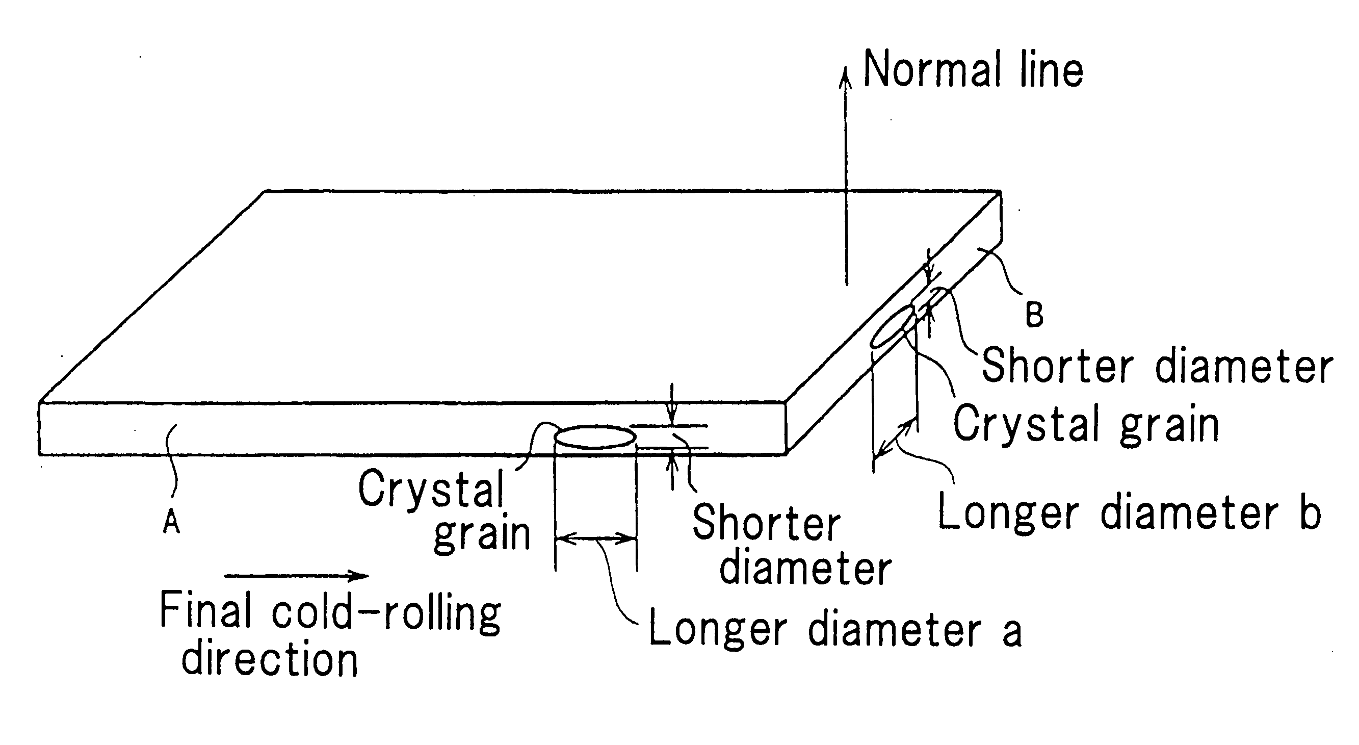
A copper alloy material for parts of electronic and electric machinery and tools contains 1.0 to 3.0 mass % of Ni, 0.2 to 0.7 mass % of Si, 0.01 to 0.2 mass % of Mg, 0.05 to 1.5 mass % of Sn, 0.2 to 1.5 mass % of Zn, and less than 0.005 mass % (including 0 mass %) of S, with the balance being Cu and inevitable impurities, wherein the copper alloy material has: (1) a specific crystal grain diameter, and a specific ratio between the longer diameters of a crystal grain on a cross section parallel or perpendicular to a direction of final plastic working; and / or (2) a specific surface roughness after the final plastic working.

Description

[0001] This is a continuation of PCT Application PCT / JP01 / 04351, filed May 24, 2001. The prior PCT application was not published in English under PCT Article 21(2).TECHNICAL FIELD [0002] The present invention relates to a copper alloy material for parts of electronic and electric machinery and tools, in particular to the copper alloy material for parts of electronic and electric machinery and tools, which is excellent in bending property and stress relaxation property, and which can sufficiently cope with miniaturization of parts of electronic and electric machinery and tools, such as terminals, connectors, switches and relays. BACKGROUND ART [0003] Hitherto, copper alloys, such as Cu—Zn alloys, Cu—Fe-alloys that are excellent in heat resistance, and Cu—Sn alloys, have been frequently used for parts of electronic and electric machinery and tools. While inexpensive Cu—Zn alloys have been used frequently, for example, in automobiles, the Cu—Zn alloys as well as Cu—Fe alloys and Cu—Sn ...

Claims


Application Information

Patent Timeline
Patent Type & Authority Applications(United States)
IPC IPC(8): B32B15/01B32B15/20C22C9/02C22C9/04C22C9/06H01H1/025H01R13/03
CPCC22C9/02C22C9/04Y10T428/12715Y10T428/12889Y10T428/12993C22C9/06
Inventor USAMI, TAKAYUKIHIRAI, TAKAO
Owner USAMI TAKAYUKI
Learn More