Method of reading multi-level nand flash memory cell and circuit for the same

a multi-level flash memory and multi-level technology, applied in digital storage, instruments, semiconductor devices, etc., can solve the problems of inability to read information of multi-level cells storing data more than two bit levels, and the multi-level sensing circuits proposed in recent years are hardly available in systems using gray codes

Active Publication Date: 2005-09-29
STMICROELECTRONICS SRL +1
View PDF6 Cites 58 Cited by
  • Summary
  • Abstract
  • Description
  • Claims
  • Application Information

AI Technical Summary

Benefits of technology

[0007] One aspect of the present invention is to provide a read circuit for a multi-level NAND flash memory cell in which comprises a cell string where plural cells for storing multi-level information are connected serially; plural word lines connected to a gate terminal of each cell string; a bit line connected to a drain terminal of the cell string; a first page buffer for storing upper-bit information among information of a cell selected by the word line and the bit line; a second page buffer for storing lower bit information of the selected cell; and a pass unit driven according to a latch pass control signal and driving the second page buffer to change information of the second page buffer.
[0008] In another aspect of the present invention, there is provided a read circuit for a multi-level NAND flash memory cell in which comprises first and second cell strings where plural cells for storing multi-level information are; connected serially; plural word lines connected to a gate terminal of each of the first and second cell strings; even and odd bit lines respectively connected to a drain terminal of the first and second cell strings; first and second bit line selection transistors selecting one of bit line among the even or odd bit line according to a bit line selection signal; a first page buffer connected to the first and second bit line selection transistors to store upper-bit information among information of a selected cell; a second page buffer connected to the first and second bit line selection transistors to store lower bit information among informati

Problems solved by technology

In general, as flash memory cells store only a single bit, there is a problem incapable of reading information of a multi-level cell storing da

Method used


Image

  • Method of reading multi-level nand flash memory cell and circuit for the same
  • Method of reading multi-level nand flash memory cell and circuit for the same
  • Method of reading multi-level nand flash memory cell and circuit for the same

Examples


Embodiment Construction

[0013] Preferred embodiments of the present invention will be described below in more detail with reference to the accompanying drawings. The present invention may, however, be embodied in different forms and should not be constructed as limited to the embodiments set forth herein. Rather, these embodiments are provided so that this disclosure will be thorough and complete, and will fully convey the scope of the invention to those skilled in the art. Like numerals refer to like elements throughout the specification.

[0014] Hereinafter, it will be described about an exemplary embodiment of the present invention in conjunction with the accompanying drawings.

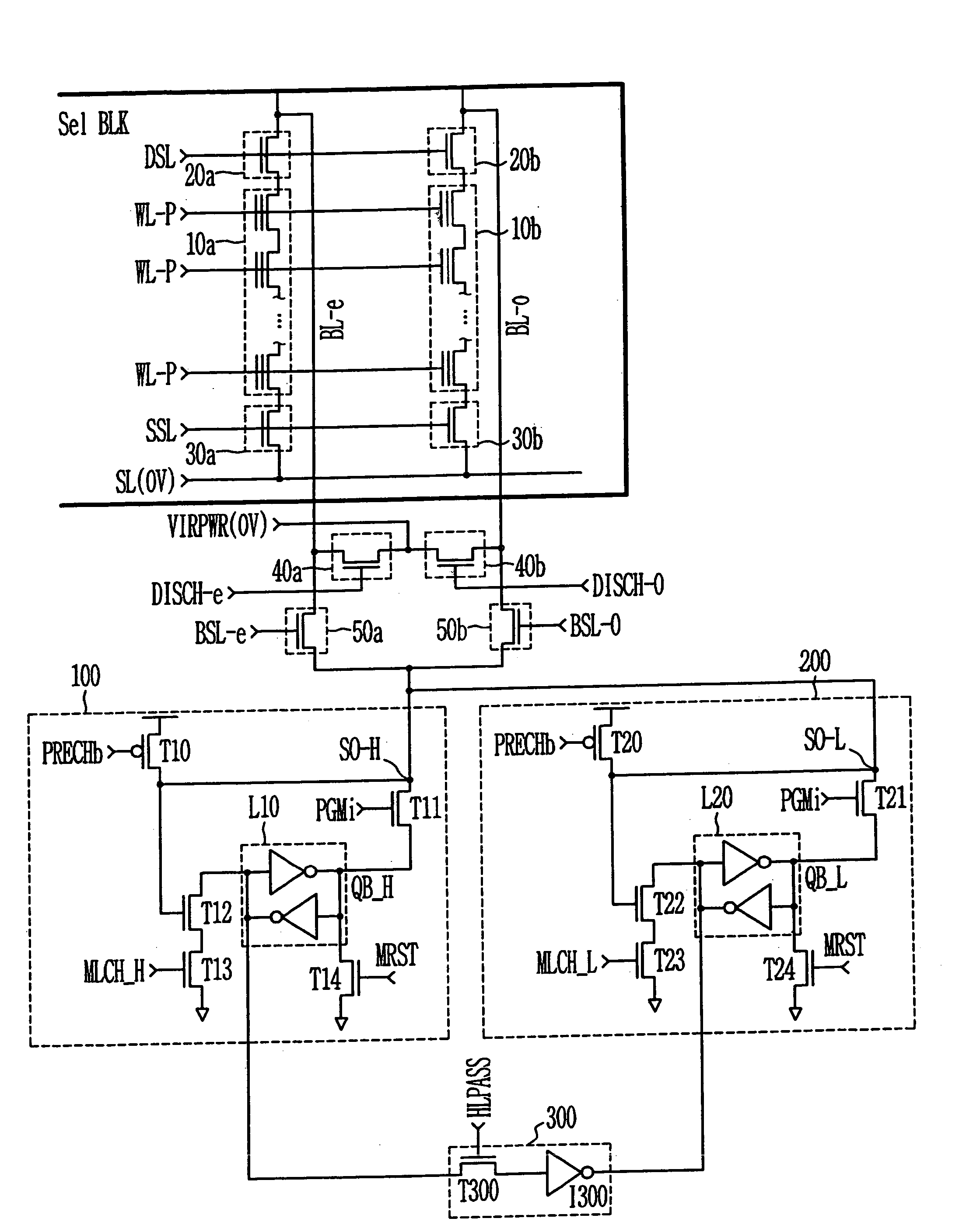
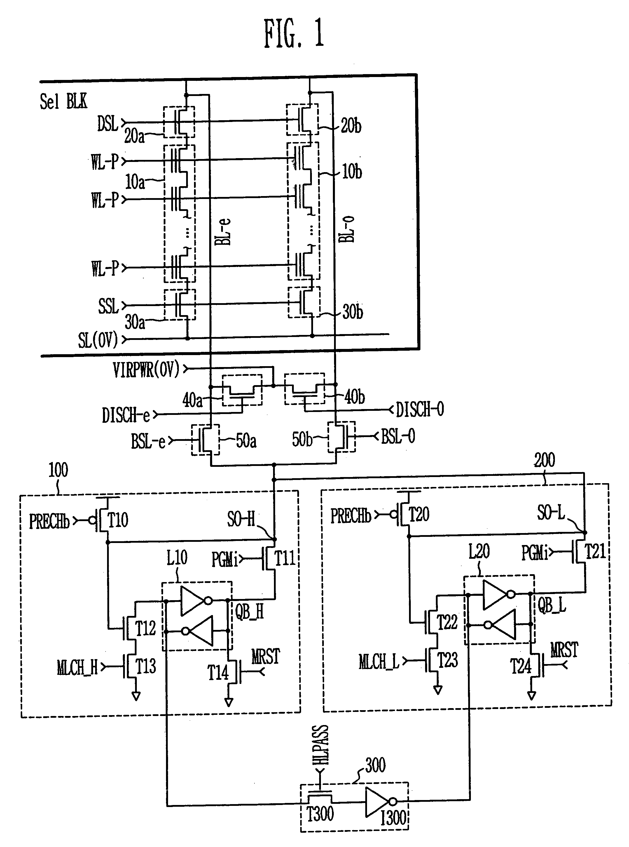
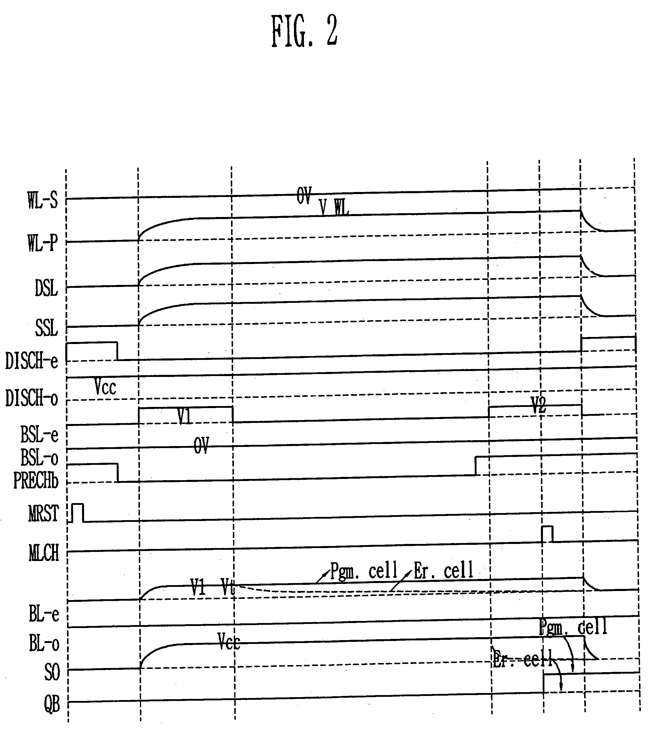
[0015]FIG. 1 is a circuit diagram of a multi-level NAND flash cell according to the present invention.

[0016] Referring to FIG. 1, a read circuit for the multi-level NAND flash cell includes a cell string 10, plural word lines WL, a bit line BL, a first page buffer 100, a second page buffer 200, and a pass unit 300. In the cell st...


PUM


Abstract

The disclosed is a method of reading a multi-level NAND flash memory cell and a circuit for the same. The read circuit for the NAND flash memory device includes a NAND flash memory cell having multi-level information, a first page buffer for storing an upper-bit, a second page buffer for storing a lower bit, and pass transistor for changing information of the second page buffer according to a variation of the first page buffer. In accordance with the present invention, “00” or “01” information is read out by applying a first voltage to a word line of the cell. “00”, “01”, or “11” information is read out by applying a second voltage to the word line. A latch pass control signal is applied to a pass transistor. Thus, it is possible to read out “00”, “01”, “11”, or “10” information.

Description

BACKGROUND [0001] 1. Field of the Invention [0002] The present invention is directed to methods of reading a multi-level flash memory and more particularly, a method of reading a multi-level flash memory used as mass data storage memory applicable in the field such as digital cameras, MP3 players etc. [0003] 2. Discussion of Related Art [0004] In general, as flash memory cells store only a single bit, there is a problem incapable of reading information of a multi-level cell storing data more than two bit levels. [0005] In addition, even multi-level sensing circuits proposed in recent are hardly available in systems using gray codes. SUMMARY OF THE INVENTION [0006] It is therefore an object of the present invention to provide a method of reading a multi-level NAND flash memory capable of using a gray code by employing a first page buffer for storing an upper-bit to a bit line and a second page buffer for storing a lower bit. [0007] One aspect of the present invention is to provide a ...

Claims


Application Information

Patent Timeline
IPC IPC(8): G11C5/02G11C16/06G11C8/12G11C11/56G11C16/02G11C16/04H01L27/115
CPCG11C8/12G11C2211/5642G11C16/0483G11C11/5642
Inventor CHANG, SEUNG HO
Owner STMICROELECTRONICS SRL
Why Eureka
Try Eureka