CMOS buffer with hysteresis
a buffer and cmos technology, applied in the field of electronic circuits, can solve the problems of noisy signal on the input of a cmos inverter that can have adverse effects on the output of the cmos inverter, and affect the operation of the digital electronics
- Summary
- Abstract
- Description
- Claims
- Application Information
AI Technical Summary
Benefits of technology
Problems solved by technology
Method used
Image

Examples
Embodiment Construction
[0018] While the present invention is described herein with reference to illustrative embodiments for particular applications, it should be understood that the invention is not limited thereto. Those having ordinary skill in the art and access to the teachings provided herein will recognize additional modifications, applications, and embodiments within the scope thereof and additional fields in which the present invention would be of significant utility.
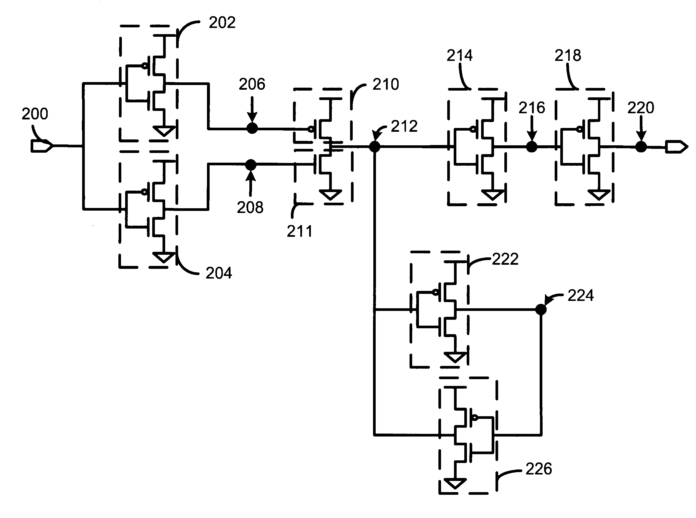
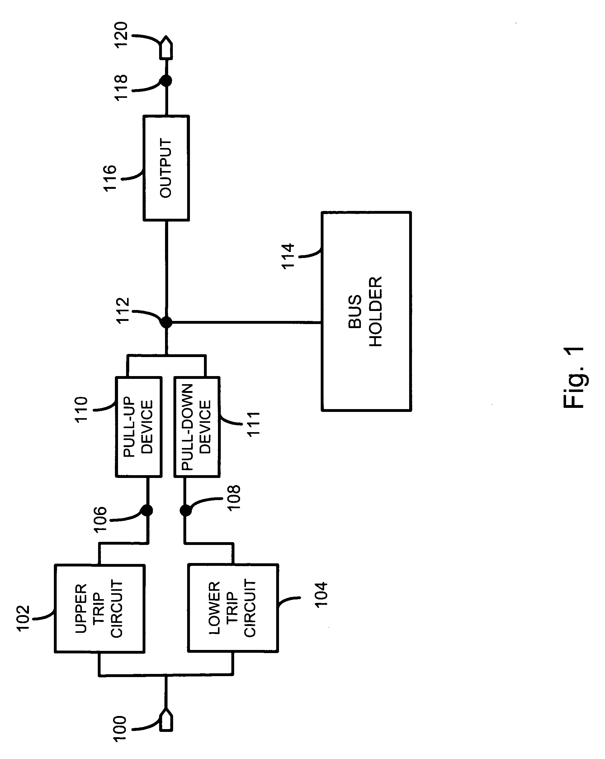
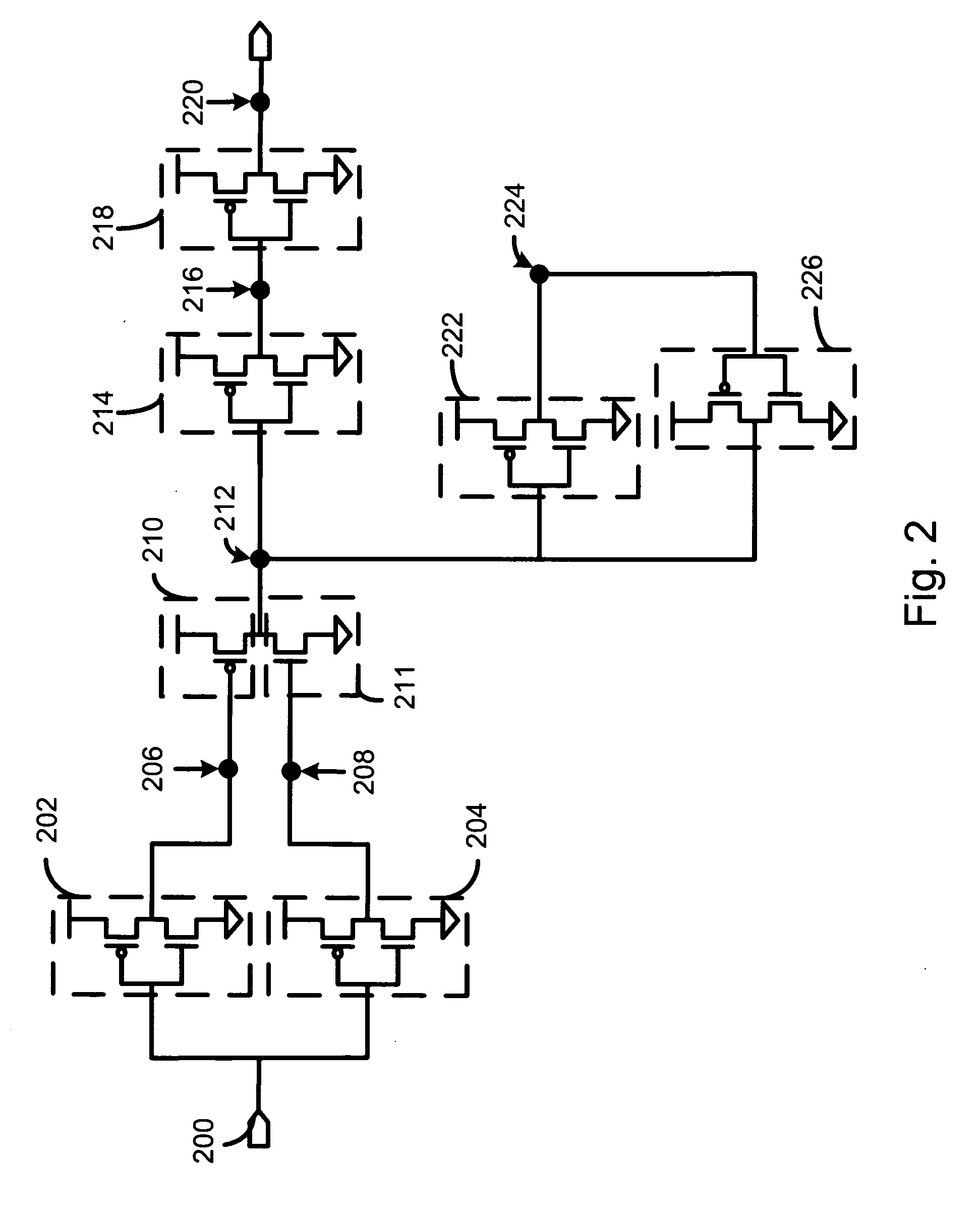
[0019]FIG. 1 displays one embodiment of the present invention. FIG. 1 displays a block diagram depiction of a circuit implemented in accordance with the teachings of the present invention. In FIG. 1, an input signal is applied to input 100. The input signal may have a rising transition or a falling transition. An upper-trip circuit 102 is connected between the input 100 and a net 106. A lower-trip circuit 104 is connected between the input 100 and a net 108. In one embodiment, the combination of the upper-trip circuit 102 and the lo...
PUM
 Abstract
Description
Claims
Application Information