Organic electronic packages having hermetically sealed edges and methods of manufacturing such packages

a technology of organic electronic packages and edges, applied in the direction of sustainable manufacturing/processing, final product manufacturing, semiconductor/solid-state device details, etc., can solve the problems of affecting the reliability of electrical contacts with organic thin films, and affecting the quality of organic thin films

Inactive Publication Date: 2005-10-13
GENERAL ELECTRIC CO
View PDF12 Cites 106 Cited by
  • Summary
  • Abstract
  • Description
  • Claims
  • Application Information

AI Technical Summary

Problems solved by technology

Disadvantageously, glass substrates are thick, heavy and relatively fragile.
Providing reliable electrical contacts to organic thin films is made more difficult when the devices are exposed to air and water, which can degrade their electronic properties rapidly.
Disadvantageously, OPVs may also be susceptible to the degradation, durability an

Method used


Image

  • Organic electronic packages having hermetically sealed edges and methods of manufacturing such packages
  • Organic electronic packages having hermetically sealed edges and methods of manufacturing such packages
  • Organic electronic packages having hermetically sealed edges and methods of manufacturing such packages

Examples


Embodiment Construction

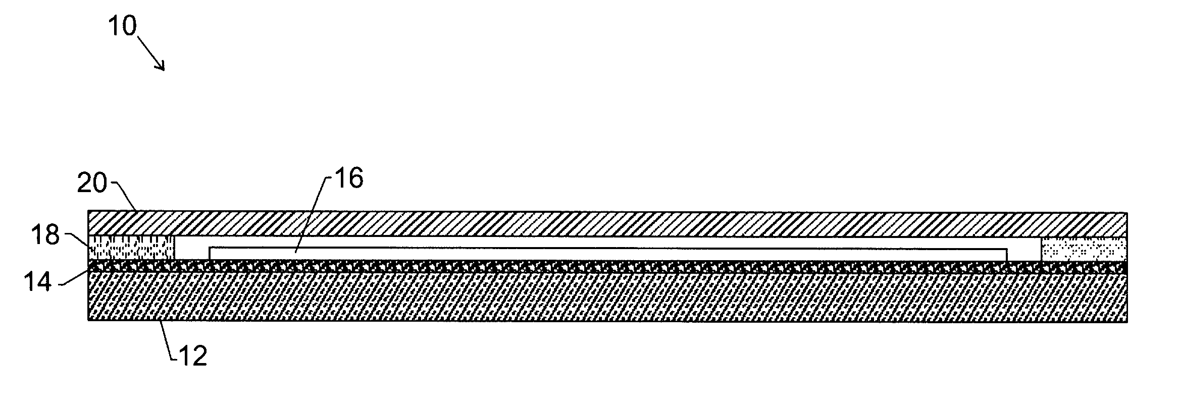
[0018]FIG. 1 illustrates an organic package having a flexible substrate 12. The flexible substrate 12 generally comprises a substantially transparent film. As used herein, “substantially transparent” refers to a material allowing a total transmission of at least about 50%, preferably at least about 80%, of visible light (i.e., having a wave length in the range from about 400 nm to about 700 nm). The flexible substrate 12 is generally thin, having a thickness in the range of approximately 0.25-50.0 mils, and preferably in the range of approximately 0.5-10.0 mils. The term “flexible” generally means being capable of being bent into a shape having a radius of curvature of less than approximately 100 cm.

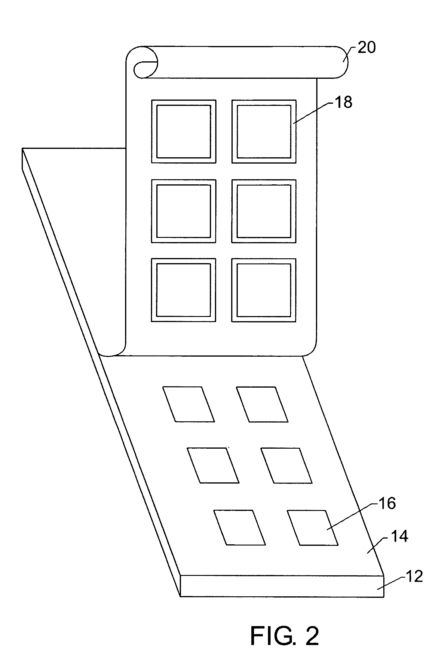
[0019] The flexible substrate 12 may be dispensed from a roll, for example. Advantageously, implementing a roll of transparent film for the flexible substrate 12 enables the use of high-volume, low cost, reel-to-reel processing and fabrication of the organic package 10. The roll of tran...


PUM


Abstract

Organic electronic packages having sealed edges. More specifically, packages having organic electronic devices are provided. A number of sealing mechanisms are provided to hermetically seal the edges of the package to completely protect the organic electronic device from external elements. A sealant may be implemented to completely surround the organic electronic device. Alternatively, edge wraps may be provided to completely surround the organic electronic device.

Description

BACKGROUND [0001] A developing trend in circuit and display technology involves the implementation of organic electronic and opto-electronic devices, which provide low cost, high performance alternatives to silicon electronic devices. One such organic device is the organic light emitting diode (OLED). OLED's are solid-state semiconductor devices, which implement organic semiconductor layers to convert electrical energy into light. Generally, OLEDs are fabricated by disposing multiple layers of organic thin films between two conductors or electrodes. The electrode layers and the organic layers are generally disposed between two substrates, such as glass or plastic. The OLEDs operate by accepting charge carriers of opposite polarities, electrons and holes, from the electrodes. An externally applied voltage drives the charge carriers into the recombination region to produce light emissions. Unlike many silicon based devices, OLEDs can be processed using low cost, large area thin film d...

Claims


Application Information

Patent Timeline
IPC IPC(8): H01L51/00H01L51/52H05B33/04
CPCH01L51/0097H01L2251/5338Y02E10/549H01L51/5246Y10T428/31504Y02P70/521H01L51/5256H01L51/5259Y02P70/50H10K77/111H10K50/846H10K50/8445H10K50/8426H10K2102/311H05B33/04H10K50/84
Inventor SCHAEPKENS, MARCDUGGAL, ANILHELLER, CHRISTIAN M.
Owner GENERAL ELECTRIC CO
Why Eureka
Try Eureka