Display apparatus and driving device for displaying

a technology of display apparatus and driving device, which is applied in the direction of differential amplifiers, amplifiers with semiconductor devices/discharge tubes, instruments, etc., can solve the problems of phase margin decrease and tendency to oscillate, and achieve the effects of suppressing eliminating a waste of steady current, and avoiding an increase in consumption power

Inactive Publication Date: 2005-10-13
RENESAS ELECTRONICS CORP
View PDF5 Cites 15 Cited by
  • Summary
  • Abstract
  • Description
  • Claims
  • Application Information

AI Technical Summary

Benefits of technology

[0009] A first object of the invention is to provide a display apparatus capable of reducing the number of parts by providing a voltage follower circuit dispensing with a stabilizing capacitor and to provide its driving device for displaying.
[0010] A second object of the invention is to provide a display apparatus capable of avoiding an increase in consumption power by suppressing charge / discharge current of a stabilizing capacitor during asymmetric drive and to provide its driving device for displaying.
[0011] A third object of the invention is to provide a display apparatus capable of suppressing an increase in consumption power by eliminating a waste of steady current flowing through a ladder resistor in match with the number of display colors and to provide its driving device for displaying.
[0013] Accordingly, to accomplish the first object, a voltage follower circuit according to an aspect of the invention comprises a differential amplifier, first and second buffer circuits, a resistor and two compensating capacitors, wherein outputs of the first and second buffer circuits are connected to each other through a resistor, the output of the first buffer circuit is fed back to one input of the differential amplifier and the output of the second buffer circuit serves as an output of the voltage follower circuit. By providing the resistor between the output of voltage follower circuit and a feedback point of the differential amplifier in this manner, the phase margin can be increased and output operation can be stabilized. At the same time, the output of the second buffer circuit can directly drive the load, thereby ensuring that the time constant can be decreased and the recovery time from voltage variations can be shortened.
[0014] To accomplish the second object, in a display apparatus according to another embodiment of the invention, voltage follower circuits for positive and negative polarities are provided and they are switched. With this construction, a potential applied to the stabilizing capacitor can be constant even in asymmetric drive of the stabilizing capacitor to thereby suppress the charge / discharge.

Problems solved by technology

When the stabilizing capacitor is supposedly removed in the general voltage follower circuit, the most critical problem is that the phase margin decreases, giving rise to a tendency to oscillation.

Method used


Image

  • Display apparatus and driving device for displaying
  • Display apparatus and driving device for displaying
  • Display apparatus and driving device for displaying

Examples


first embodiment

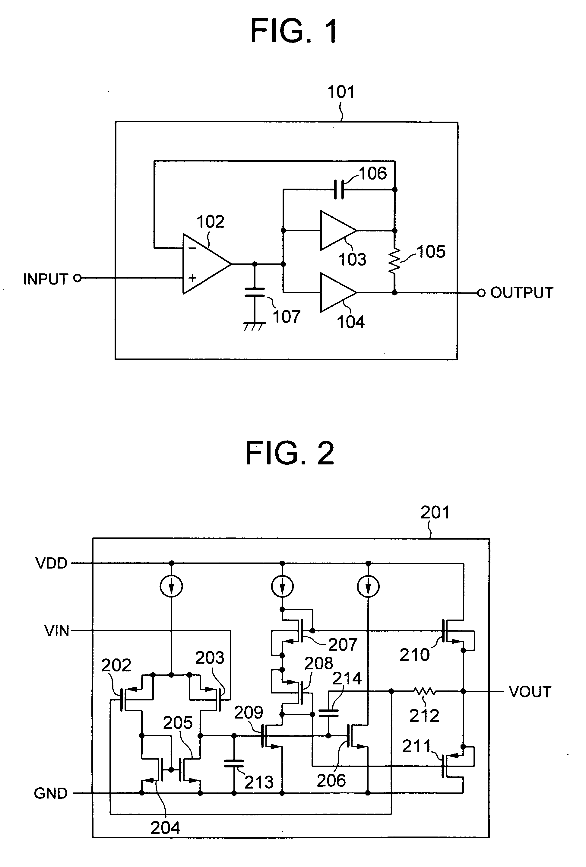
[0029]FIG. 1 illustrates the fundamental construction of a voltage follower circuit according to the invention. The voltage follower circuit, as designated at reference numeral 101, in the present embodiment comprises a differential amplifier 102, first and second buffer circuits 103 and 104, a resistor 105 and two compensating capacitances (for example, capacitors) 106 and 107. This circuit construction is featured in that outputs of the first and second buffer circuits 103 and 104 are connected to each other through the resistor 105, with the output of first buffer circuit 103 being fed back to one input of the differential amplifier 102 and the output of the second buffer circuit 104 being connected to serve as an output of the voltage follower circuit 101. By providing the resistor 105 between the output of voltage follower circuit 101 and a node for feedback to the differential amplifier 102 in this manner, the phase margin can be increased to stabilize output operation. In add...

second embodiment

[0044]FIG. 8 illustrates a circuit diagram showing the construction of a gray scale voltage generating circuit according to the invention. The circuit comprises switches for switching gray scale voltages for positive and negative polarities, a ladder resistor 803 for generating gray scale voltages for positive polarity, and a ladder resistor 804 for generating gray scale voltages for negative polarity. Other components are identical to those of the gray scale voltage generating circuit 401 shown in FIG. 4. This circuit construction is featured in that there are provided two kinds of ladder resistors 803 and 804 for positive and negative polarities and two kinds of voltage follower circuits 402 and 408 for positive polarity and voltage follower circuits 403 and 409 for negative polarity and that switches are provided which respond to an A.C. signal from the liquid crystal controller to switch the two kinds of ladder resistors and the two kinds of voltage follower circuits. In connect...

fourth embodiment

[0046]FIG. 10 illustrates a circuit diagram showing the construction of a gray scale voltage generating circuit according to the invention. The circuit comprises resistors 1001 for positive polarity, resistors 1002 for negative polarity, and switches 1003 each adapted to selectively switch connection between a ladder resistor for generation of reference voltages and each of the resistors 1001 and 1002 for positive and negative polarities. The circuit construction shown in FIG. 10 intends to singularize the ladder resistor for generation of reference voltages. Specifically, any one of the ladder resistors 803 and 804 in the gray scale voltage generating circuit shown in FIG. 8 can be unneeded. Namely, by making resistance of the resistor 1001 different from that of the resistor 1002, gray scale voltages at different levels can be generated at positive and negative polarities. This construction is preferably applied to upper and lower ends of the ladder resistor so as to enhance the d...


PUM

PropertyMeasurementUnit
frequencyaaaaaaaaaa
gray scale voltageaaaaaaaaaa
voltagesaaaaaaaaaa

Abstract

A display drive circuit for outputting a gray scale voltage according to display data includes a generation circuit generating gray scale voltages of a plurality of levels, and a selection circuit which selects a gray scale voltage according to the display data. When the number of colors to be displayed is small, the generation circuit decreases a current flowing into an internal circuit which generates a gray scale voltage of an intermediate level other than two gray scale voltages of a gray scale voltage of the most lowest level and a gray scale voltage of the most highest level among the gray scale voltages of the plurality of levels, and the selection circuit selects the gray scale voltage according to the display data from the most lowest level gray scale voltage and the most highest level gray scale voltage which are generated.

Description

CROSS REFERENCE TO RELATED APPLICATION [0001] This is a continuation of U.S. application Ser. No. 10 / 918,379, filed Aug. 16, 2004, which is a continuation of U.S. application Ser. No. 10 / 161,638, filed Jun. 5, 2002, now U.S. Pat. No. 6,781,605, the subject matter of which is incorporated by reference herein.BACKGROUND OF THE INVENTION [0002] The present invention relates to a display apparatus having a display panel in which display pixels are arranged in matrix and a driving device for displaying adapted to deliver the display panel gray scale voltages matching with display data and more particularly to, a display apparatus using liquid crystal, organic EL, plasma or the like and a driving device for displaying adapted for use in the same. [0003] JP-A-6-348235 discloses a liquid crystal panel having X-signal lines and Y-signal lines, a horizontal driver for selecting, on the basis of a data signal of an image to be displayed, one gray scale signal from a plurality of gray scale sig...

Claims


Application Information

Patent Timeline
Patent Type & Authority Applications(United States)
IPC IPC(8): G02F1/133G09G3/00G09G3/20G09G3/30G09G3/36G09G5/00H03F3/347H03F3/45
CPCG09G3/20H03F3/45475G09G3/2092G09G3/3614G09G3/3688G09G3/3696G09G2310/027G09G2320/0626G09G2320/066G09G2320/08G09G2330/021G09G2330/028G09G2360/18H03F3/347G09G3/2011
Inventor KUDO, YASUYUKIAKAI, AKIHITOOOKADO, KAZUOKUROKAWA, KAZUNARIHIGA, ATSUHIRO
Owner RENESAS ELECTRONICS CORP
Why Eureka
Try Eureka