Chip card of reduced size with backward compatibility and adapter for a reduced size chip card

Active Publication Date: 2005-10-20
NTT DOCOMO INC
View PDF9 Cites 77 Cited by
  • Summary
  • Abstract
  • Description
  • Claims
  • Application Information

AI Technical Summary

Benefits of technology

[0018] In view of the above, an object of the present invention is to achieve backward compatibility for sma

Problems solved by technology

One problem with available solutions is that the ID-000 format more and more restricts mobile terminal design, as the size of these mobile terminals becomes smaller and smaller.
Another problem in view of the introduction of smaller chip cards into the mobile communication network market is inter-operability with existing chip card readers/writers, e.g., for initialisation and personalization when the chip card is issued or passed to the end user, and further inter-operability with mobile terminals.
In particular, backward compatibil

Method used


Image

  • Chip card of reduced size with backward compatibility and adapter for a reduced size chip card
  • Chip card of reduced size with backward compatibility and adapter for a reduced size chip card
  • Chip card of reduced size with backward compatibility and adapter for a reduced size chip card

Examples


Embodiment Construction

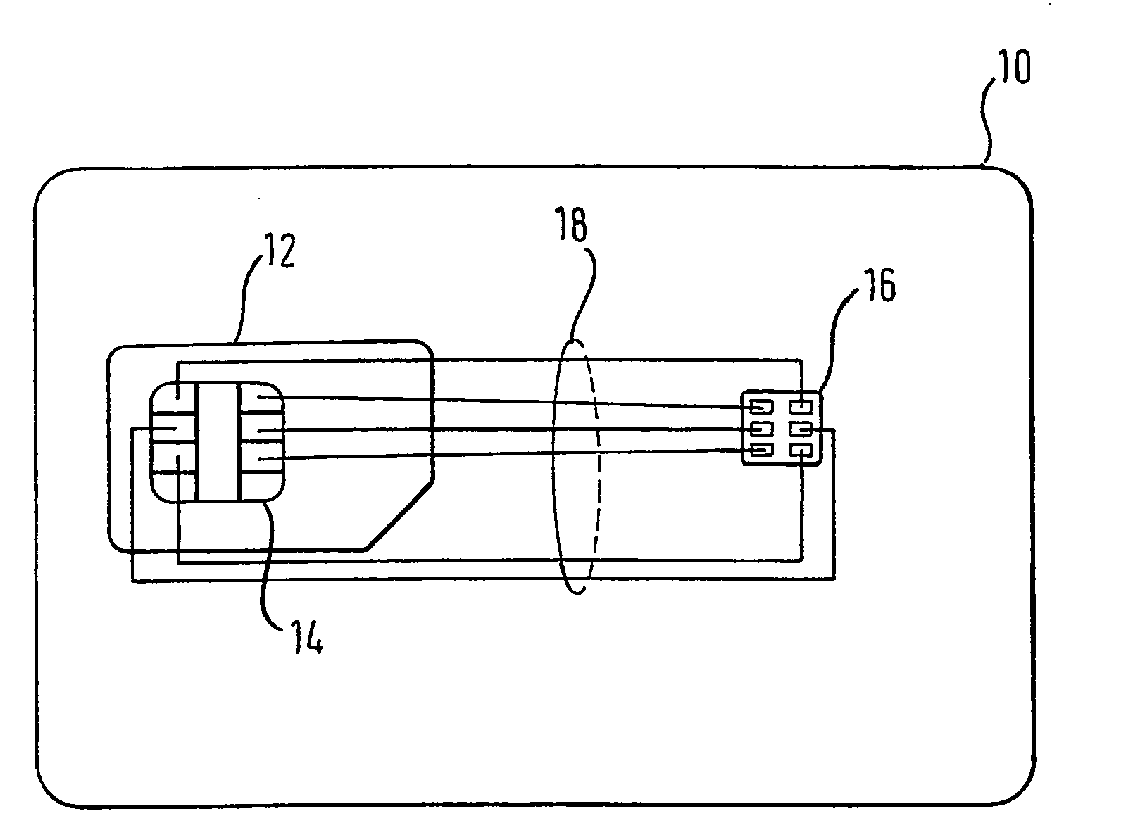
[0071] In the following preferred embodiments of the present invention will be described with reference to the drawings.

[0072] Heretofore, reference will be made to smaller chip cards.

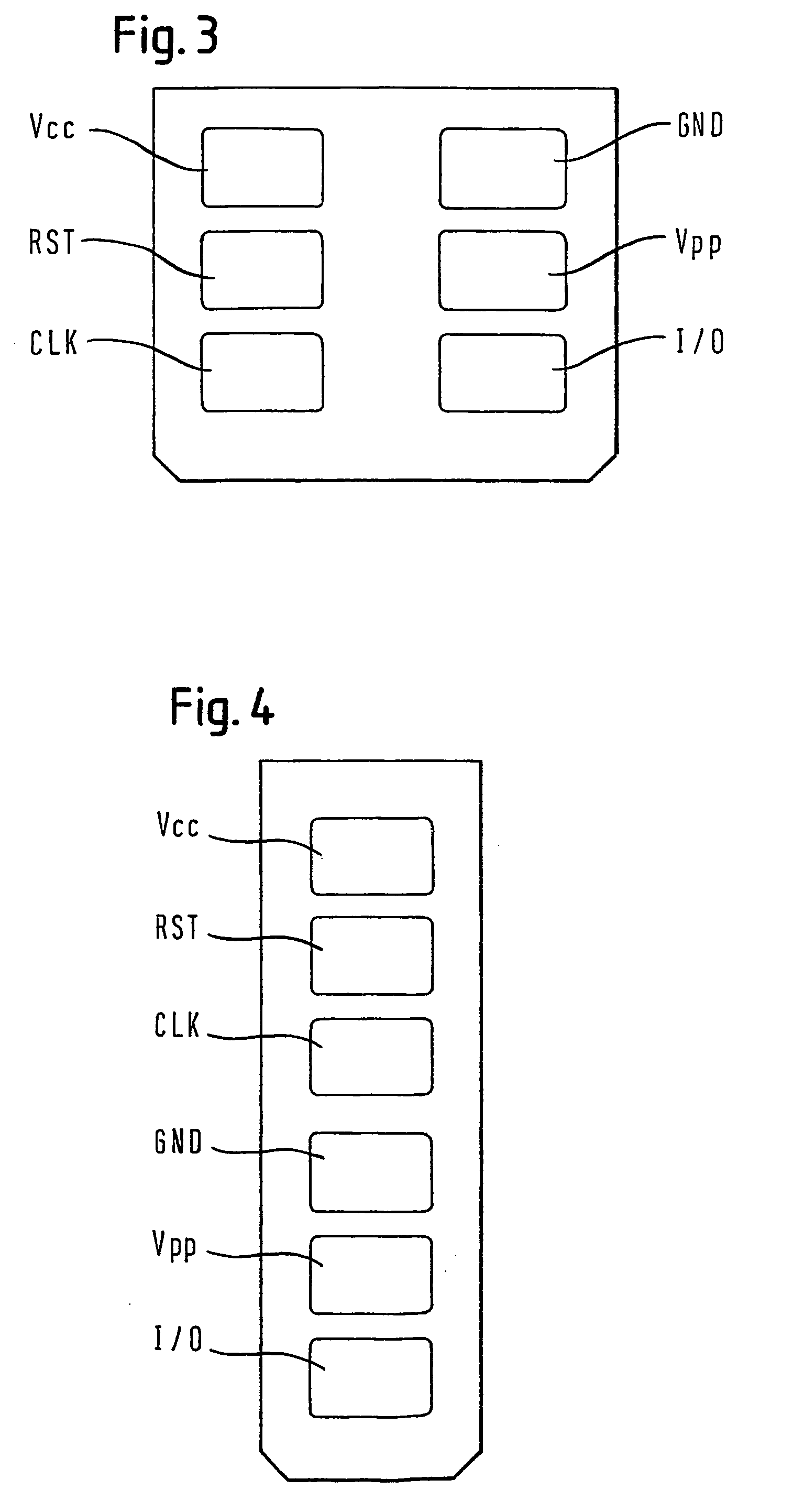
[0073] A first example for a smaller chip card having dimensions smaller than ID-000 or in other words close to silicon is shown in FIG. 3. Different contacts are arranged along two parallel lines. E.g., the contacts are used for voltage supply Vcc, reset input RST, clock CLK, ground GND, program voltage Vpp, input / output for serial communication I / O. Of course, the ordering of the contacts along the lines may be permutated or one or more contact(s) may be omitted or added.

[0074] A second example for a smaller chip card having dimensions close to silicon is shown in FIG. 4. The smaller chip card differs from the smaller chip card shown in FIG. 3 in that contacts are arranged a single line only. Again, the indicated use of contacts is to be considered as an example for the present invention only and ...


PUM


Abstract

To achieve backward compatibility for smaller chip cards, in particular to legacy card readers/writers or legacy mobile terminals, according to the present invention a smaller chip card comprises a card body and a first contact area (14) with dimensions and locations of contacts according to predefined standard. An integrated circuit chip (36) is, firstly, physically and electrically connected to contacts of a second contact area (38), where the locations of contacts in the second contact area (38) are different from locations of contacts in the first contact area (14). According to the present invention, the integrated circuit chip (36) is also connected to contacts in the first contact area (14).

Description

FIELD OF INVENTION [0001] The present invention relates to a smaller chip card, and in particular to a smaller chip card with backward compatibility and an adaptor for portability of the smaller chip card. BACKGROUND OF INVENTION [0002] Patent abstracts of Japan, vol. 016, no. 440 (M-1310), 14 Sep. 1992 and JP 04 153097 relate to the provision of two IC chips which are arranged mutually symmetrically on a chip card, wherein the symmetry is achieved with respect to the insertion direction. This allows to enhance safety of operation. [0003] DE 199 26 348 A describes a method for manufacturing of mini chip cards and the related arrangement of two mini chip cards on a bearer card, e.g., according to the ID-1 format. [0004] DE 199 22 063 A describes an adapter card in a communication device for a chip card having a means for inserting of a chip card and further an identification means for the chip card. The identification means serves to select the appropriate bus, operative voltage or o...

Claims


Application Information

Patent Timeline
IPC IPC(8): G06K7/00B42D15/10G06K17/00G06K19/06G06K19/077
CPCG06K7/0021G06K19/072G06K19/07733H01L2224/48095G06K19/07743G06K19/07741H01L2924/00014
Inventor NODA, CHIEMURASE, ATSUSHIISHIKAWA, HIDETOSHI
Owner NTT DOCOMO INC
Why Eureka
Try Eureka