Flash memory cell structure and operating method thereof

Active Publication Date: 2005-10-20
POWERCHIP SEMICON MFG CORP
View PDF4 Cites 2 Cited by
  • Summary
  • Abstract
  • Description
  • Claims
  • Application Information

AI Technical Summary

Benefits of technology

[0013] Moreover, the claimed invention provides an operation method applied to the flash memory cell structure. In the claimed invention, when executing a programming process a high voltage is applied to the control gate, a voltage relatively lower than the control gate voltage is applied to the drain, the source is floating, and the select gate is grounded. When executing an erasing process, a low voltage is applied to the control gate, a voltage relatively higher than the control gate voltage is applied to the select gate, and the source and the drain are floating. When executing a r

Problems solved by technology

In that case, the lateral electric field will result in hot hole injection, and will seriously affect normal operation of the flash memory cell structure 1.
Although employing the channel Fowler-Nordheim effect in the foregoing flash memory cell structure can overcome drawbacks, this may result in other problems.
However, it is not easy to control the thickness in the manufacturing process, and the reliability will be further reduced.
Furthermore, the flash memory cell structure adjacent to the flash memory cell structure 2 has leakage problems when the flash memory cell structure 2 is programmed.
If a negative voltage is not applied, the charging pumping will increase, which could further cause a malfunction of the flash memory cell structure.

Method used


Image

  • Flash memory cell structure and operating method thereof
  • Flash memory cell structure and operating method thereof
  • Flash memory cell structure and operating method thereof

Examples


Embodiment Construction

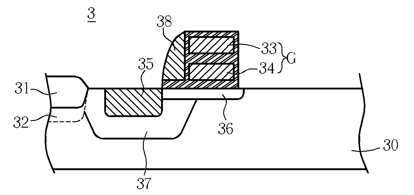
[0025] Please refer to FIG. 4, which is a schematic diagram illustrating a flash memory cell structure 3 according to a preferred embodiment of the present invention. As shown in FIG. 4, the flash memory cell structure 3 includes a substrate 30, a first-type doped region 35, a shallow second-type doped region 36, a deep second-type doped region 37, and a select gate 38.

[0026] In this preferred embodiment, the substrate 30 includes a first field oxidation layer 31 and a stacked gate G. A channel stop 32 is formed underneath the first field oxidation layer 31, the stacked gate G further includes a control gate 33 and a floating gate 34, and the select gate 38 is formed on a side of the stacked gate G.

[0027] The first-type doped region 35 is formed in the substrate 30 and adjacent to the select gate 38 as a drain. The first-type doped region 35 can be an N type doped region in this embodiment.

[0028] The shallow second-type doped region 36 is located underneath the stacked gate G and...


PUM


Abstract

A flash memory cell structure has a substrate, a select gate, a first-type doped region, a shallow second-type doped region, a deep second-type doped region, and a doped source region. The substrate has a stacked gate. The select gate is formed on the substrate and adjacent to the stacked gate. The first-type ion formed region is doped in the substrate and adjacent to the select gate as a drain. The shallow second-type doped region is formed on one side of the first-type doped region below the stacked gate. The deep second-type doped region, which serves as a well, is formed underneath the first-type doped region with one side bordering on the shallow second-type doped region. The doped source region is formed on a side of the shallow second-type doped region as a source.

Description

CROSS REFERENCE TO RELATED APPLICATIONS [0001] This application is a divisional of application Ser. No. 10 / 605,419 filed Sep. 30, 2003.BACKGROUND OF THE INVENTION [0002] 1. Field of the Invention [0003] The present invention relates to a non-volatile memory cell structure, and more particularly, to a flash memory cell structure and an operating method thereof. [0004] 2. Description of the Prior Art [0005] Refer to FIG. 1. A prior art flash memory cell structure 1 includes a substrate 10, a drain 11, a source 12, two field oxidation layers 13, a control gate 14, a floating gate 15, and a P well 16. The drain 11 and the source 12 are formed in the substrate 10 and between the field oxidation layers 13. A stacked gate, which includes the control gate 14 and the floating gate 15, is between the drain 11 and the source 12. Further, the P well 16 is implanted around the drain 11 and the source 12. As shown in FIG. 1, a gate voltage VG is applied to the control gate 14 for controlling the ...

Claims


Application Information

Patent Timeline
IPC IPC(8): G11C16/04H01L21/28H01L21/336H01L29/423H01L29/788
CPCG11C16/0425H01L21/28273H01L29/7885H01L29/66825H01L29/42328H01L29/40114
Inventor HUNG, CHIH-WEISUNG, DAHSU, CHENG-YUAN
Owner POWERCHIP SEMICON MFG CORP
Why Eureka
Try Eureka