Wafer-level optical structure

a technology of optical structure and fiber, applied in the direction of adhesive process using foamed adhesives, instruments, radiation control devices, etc., can solve the problems of contaminating neighbor regions, overgluing, severe problems, etc., and achieve optimal optical performance and product quality. good

Active Publication Date: 2020-04-28
HIMAX TECH LTD
View PDF9 Cites 0 Cited by
  • Summary
  • Abstract
  • Description
  • Claims
  • Application Information

AI Technical Summary

Benefits of technology

[0027]The novel method to form a wafer-level optical structure of the present invention forms a trench to accommodate the spacer which supports the optically transparent substrate and to accommodate the soft adhesive material which is used to permanently fix the spacer. In such a way, the soft, liquid-like adhesive material before curing is well accommodated inside the trench so the over-flow problem or the over-glue issue can be greatly improved or completely solved.
[0028]Further, the adhesive material may be cured in the absence of a thermal treatment to eliminate an undesirable bow distortion of the optically transparent wafer along with the polymeric layer and the undesirable misalignment of stack layers to overcome the misalignment problems in prior art. Accordingly, the obtained novel wafer-level optical structure has neither undesirable bow distortion, neither undesirable misalignment of stack layers, nor undesirable over-flow problem and over-glue issue to show better product quality and optimal optical performance.

Problems solved by technology

When the soft, liquid-like adhesive is squeezed by the spacers after the soft, liquid-like adhesive is first applied to the lens layer, it would induce a severe problem.
Due to the top-down pressure, the soft, liquid-like adhesive overflows to the neighbor region to cause over-glue issue and simultaneously contaminates the neighbor region.
A wafer-level optical structure with the over-flow problem or with the over-glue issue apparently shows bad optical quality.

Method used


Image

  • Wafer-level optical structure
  • Wafer-level optical structure
  • Wafer-level optical structure

Examples


Embodiment Construction

[0046]To eliminate undesirable bow distortion, undesirable misalignment of stack layers, or undesirable over-flow problem and over-glue issue, the present invention provides a novel method to form an optical structure on a wafer-level scale. The novel method of the present invention proposes a solution to accommodate the soft, liquid-like uncured adhesive material which is used to permanently fix the spacers to improve the over-flow problem and over-glue problem. Further, the adhesive material may be cured in the absence of a thermal treatment to eliminate the undesirable bow distortion of the optically transparent wafer along with the polymeric layer and the undesirable misalignment of stack layers to exhibit better product quality, interlayer alignment accuracy and optical performance.

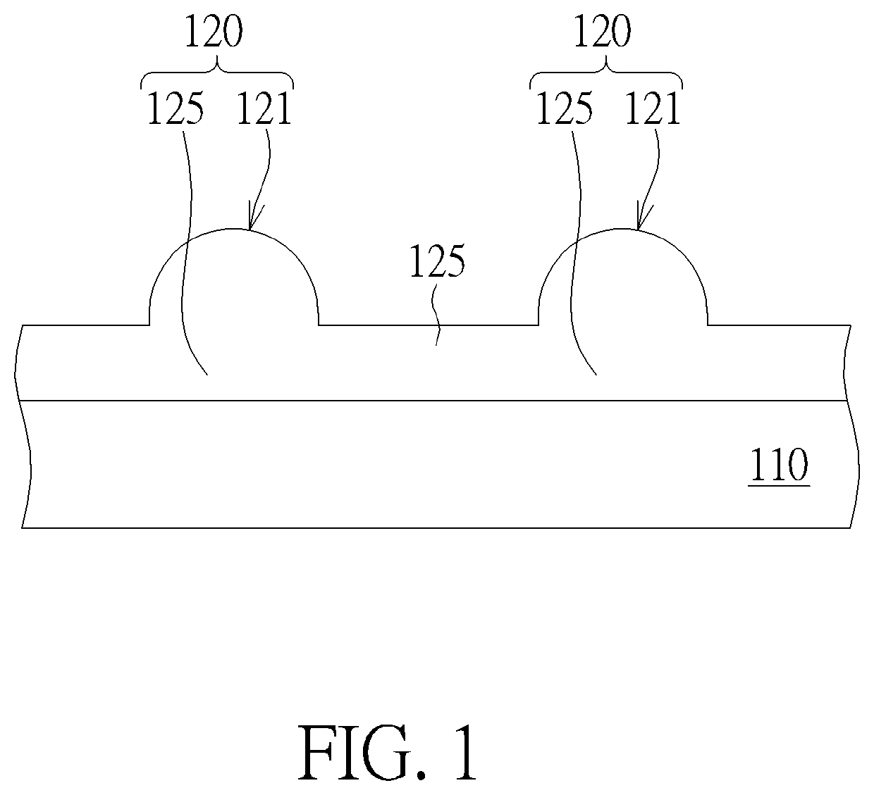
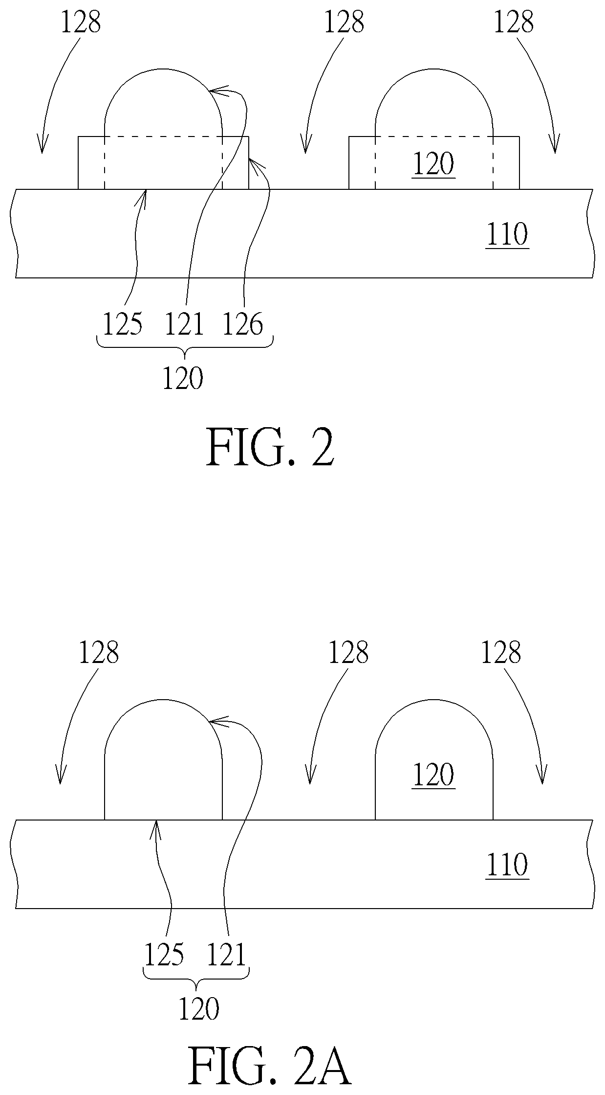
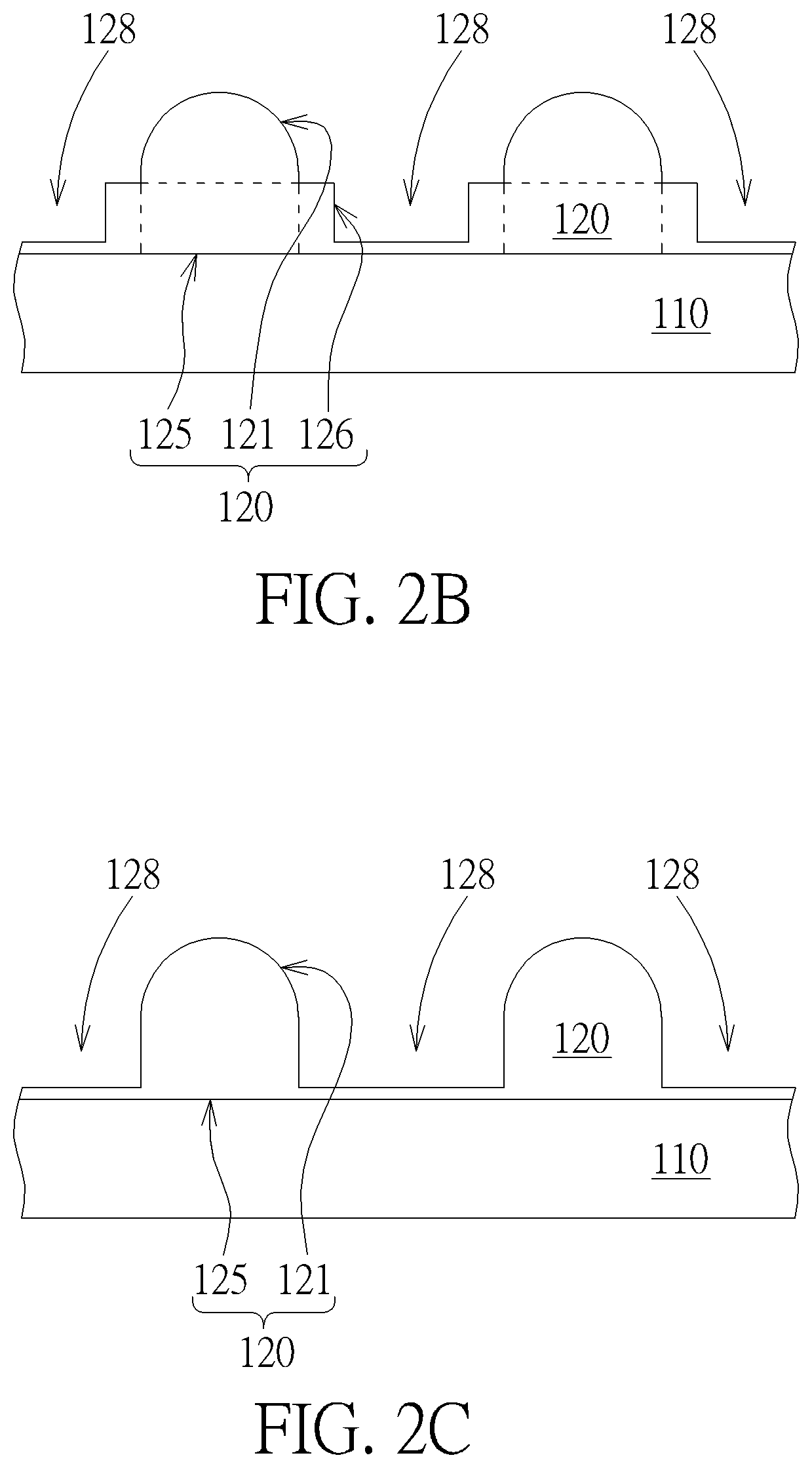
[0047]FIG. 1 to FIG. 6 illustrate a first example of a novel method to form a wafer-level optical structure of the present invention. Please refer to FIG. 1. First, an optically transparent wafer 110...


PUM

PropertyMeasurementUnit
diameteraaaaaaaaaa
widthaaaaaaaaaa
widthaaaaaaaaaa

Abstract

A wafer-level optical structure includes at least two optical lens sets disposed on an optically transparent wafer, at least one trench disposed between two adjacent optical lens sets to divide the two adjacent optical lens sets, at least one spacer disposed between two adjacent optical lens sets to be correspondingly and partially disposed in the trench, and an adhesive disposed inside the trench.

Description

BACKGROUND OF THE INVENTION1. Field of the Invention[0001]The present invention generally relates to a wafer-level optical structure as well as to a method to forma wafer-level optical structure. In particular, the present invention is directed to a wafer-level optical structure which is free of an over-flow problem or free of an over-glue issue to overcome some problems in prior art. The present invention is also directed to a method to form a wafer-level optical structure in the absence of the over-flow problem or of the over-glue issue to overcome the current problems in prior art.2. Description of the Prior Art[0002]In addition to fabricate optical lens sets which are required to be assembled individually from a multitude of individual parts, it is also possible to fabricate a large area of optical lens sets at the same time on an optical glass wafer alternatively in accordance with the conventional semiconductor manufacture process. This top-tier technology is known as “wafer-l...

Claims


Application Information

Patent Timeline
Patent Type & Authority Patents(United States)
IPC IPC(8): H01L31/062H01L27/146H04N5/225C09J5/08
CPCH01L27/14632C09J5/08H01L27/14627H01L27/14687H04N5/2254G02B3/00H01L27/14621H04N23/55
Inventor CHANG, CHIH-SHENGHUANG, TENG-TEHSU, SHU-HAOZHAN, JUN-YU
Owner HIMAX TECH LTD
Why Eureka
Try Eureka