Scanning electron microscope

a scanning electron microscope and microscope technology, applied in material analysis using wave/particle radiation, instruments, nuclear engineering, etc., to prevent erroneous correction, reduce the moving distance between the selected defects, and improve the inspection speed

Active Publication Date: 2005-10-27
HITACHI HIGH-TECH CORP
View PDF12 Cites 9 Cited by
  • Summary
  • Abstract
  • Description
  • Claims
  • Application Information

AI Technical Summary

Benefits of technology

[0018] For correcting the coordinate value of a defect, it is possible to prevent erroneous correction at the initial stage and thereby correct a coordinate value of a defect so that the erroneous correction may be reduced and the defect may be w

Problems solved by technology

Hence, around the center of the wafer, the offset error caused by the shift of the installing p

Method used


Image

  • Scanning electron microscope
  • Scanning electron microscope
  • Scanning electron microscope

Examples


first embodiment

[First Embodiment]

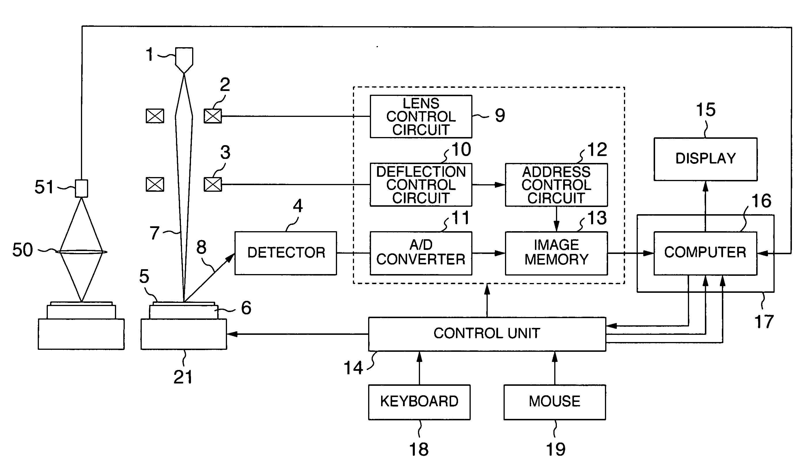
[0027] Hereafter, the embodiment of the present invention will be described in detail with reference to the accompanying drawings. FIG. 1 shows an arrangement of an SEM according to the first embodiment of the invention. Though the description will be expanded with the SEM as an example, the image of an optical imaging device may be used for this arrangement. In this case, a bright field optical system image or a dark field optical system may be used therefor. Moreover, it is possible to selectively use these images. For example, when first specific points are selected, the bright field or the dark field optical system image may be used. Later, the SEM image may be used. In this case, by using the image of the optical system imaging device with a wide image area, the first great offset between the coordinate systems may be executed more effectively and for a shorter time. The optional combination of them is made possible.

[0028] The SEM shown in FIG. 1 is arranged ...

second embodiment

[Second Embodiment]

[0055] The method of selecting defects shown in the steps S5, S6, S10 and S11 may be changed as follows. This changed method is shown in the flowchart of FIG. 6.

[0056] In FIG. 6, the process of the steps S1 to S3 is executed at first. This is the same as the process of the steps S1 to S3 included in the first embodiment. Hence, the details of the process is left out.

[0057] Proceeding to a step S13, the process is executed to set a boundary line surrounding the center of a wafer as shown in FIG. 7 and divide the wafer surface into a plurality of areas. Each boundary line is closed and is not crossed with another boundary line. As an example, FIG. 7 shows four concentric boundary lines 81 with the center of the wafer set as the center of the circle and five areas 82 to 86 of the wafer divided by these four boundary lines 81. The method of division and the form are not limited to those shown in FIG. 7.

[0058] In the following step S14, the process is executed to se...


PUM


Abstract

This SEM has a capability of preventing shift of a view field of the foreign matters at a stage where no sufficient correction is carried out when obtaining the SEM coordinate values used for transforming the coordinate values of the foreign matters on the sample sent from another device into the SEM coordinate values. The SEM selects the foreign matters closer to the center of the sample at first and then the foreign matters spirally from the center of the sample to the outer periphery.

Description

BACKGROUND OF THE INVENTION [0001] 1. Field of the Invention [0002] The present invention relates to a scanning electron microscope which enables to observe a fine object to be measured, the object being located on the surface of a sample. More particularly, the present invention relates to the scanning electron microscope which is arranged to transform the coordinate data of an object to be observed, the object being located on a sample measured by another foreign matter inspector into the data fitted for the coordinate system of itself and then to utilize the converted data when observing an object. [0003] 2. Description of the Related Art [0004] A scanning Electron Microscope (often but not always referred to as an SEM) is used for observing a fine structure of a sample in various fields of research and development. The SEM operates to display on screen an SEM image of an object to be observed when observing the object. This technology is applied to observation of a microstructur...

Claims


Application Information

Patent Timeline
IPC IPC(8): H01J37/28G01N23/00G21K7/00
CPCH01J37/265H01J2237/2817H01J37/28
Inventor YAMAGUCHI, KOHEIAOKI, KAZUOISOGAI, SEIJISAKAMOTO, MASASHI
Owner HITACHI HIGH-TECH CORP
Why Eureka
Try Eureka