Asymmetric pattern projection apparatus

a projection apparatus and asymmetric pattern technology, applied in the direction of instruments, material analysis, television systems, etc., can solve the problems of prohibitive cost increase and expensive approach, and achieve the effect of improving the inspection speed, reducing the fov of the inspection device, and sacrificing the accuracy of height measuremen

Active Publication Date: 2013-01-24
ASMPT SINGAPORE PTE LTD
View PDF4 Cites 6 Cited by
  • Summary
  • Abstract
  • Description
  • Claims
  • Application Information

AI Technical Summary

Benefits of technology

[0006]It is thus an object of the invention to seek to provide an inspection apparatus which increases the FOV of an inspection device without significantly sacrificing the height measurement accuracy therein in order to improve its inspection speed.

Problems solved by technology

However, increasing the inspection speed can be achieved by increasing the size of FOV, but it will be an expensive approach if height measurement accuracy is not to be sacrificed.
That is because it requires a larger CCD sensor, optical lenses with larger diameters, larger size of the whole inspection module as well as larger supports for this module in the machine, all of which lead to prohibitive increases in cost.

Method used


Image

  • Asymmetric pattern projection apparatus
  • Asymmetric pattern projection apparatus
  • Asymmetric pattern projection apparatus

Examples


Embodiment Construction

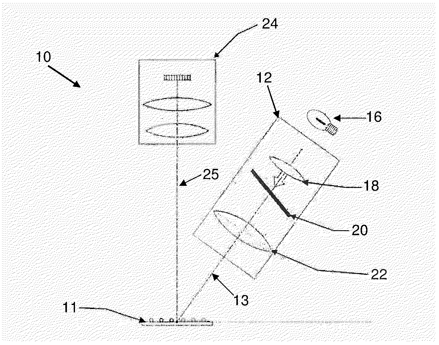
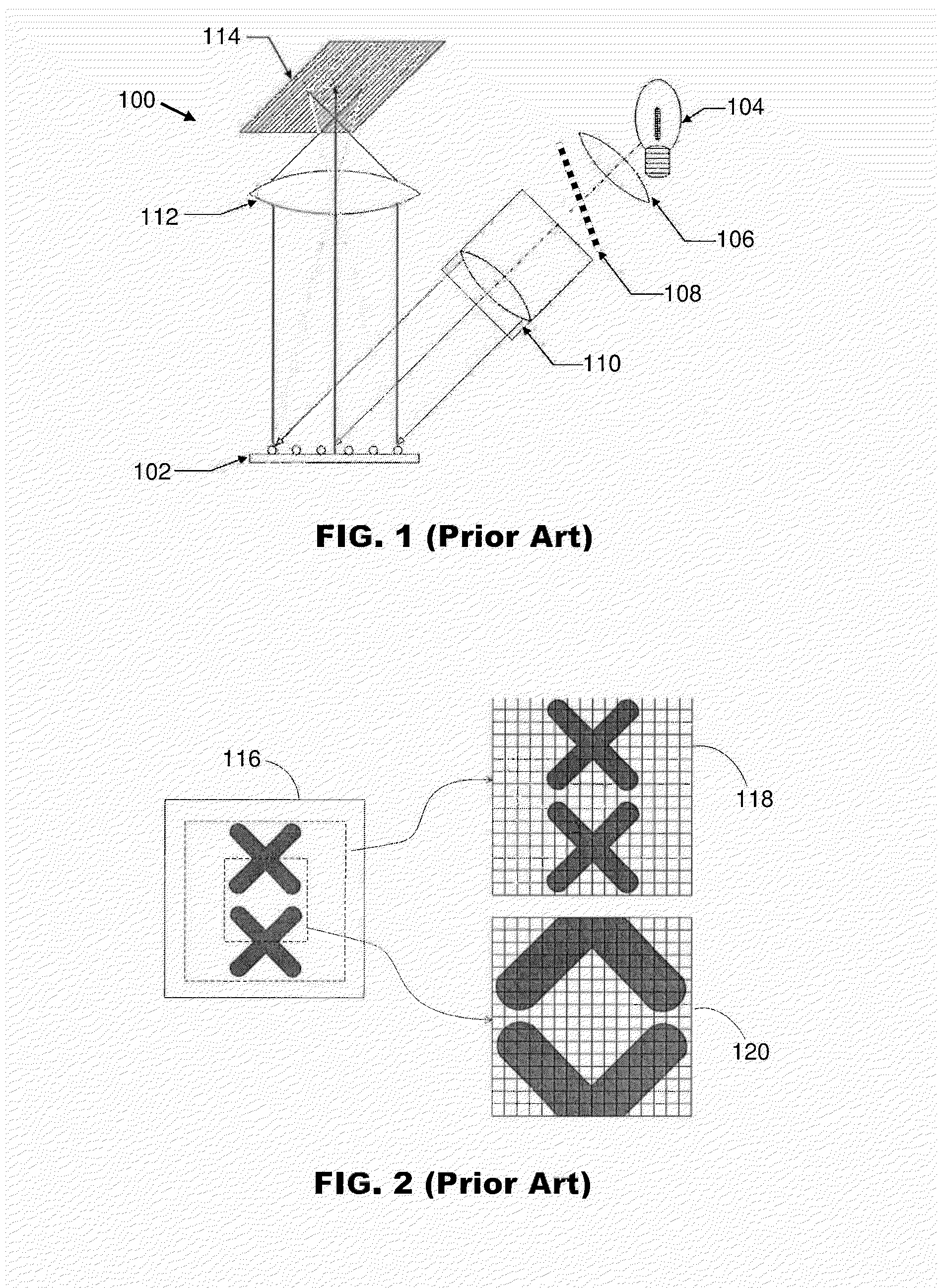
[0020]By way of illustration, FIG. 1 is a conventional layout of a pattern projection system 100 for three-dimensional measurement. The pattern projection system 100 includes a pattern production part which comprises a light source 104, condenser 106, grating 108 and lenses 110 to project a grating image onto a device 102 which is to be measured. The pattern projection system 100 also includes an imaging part which comprises lenses 112 to focus a formed image 114 onto an image plane.

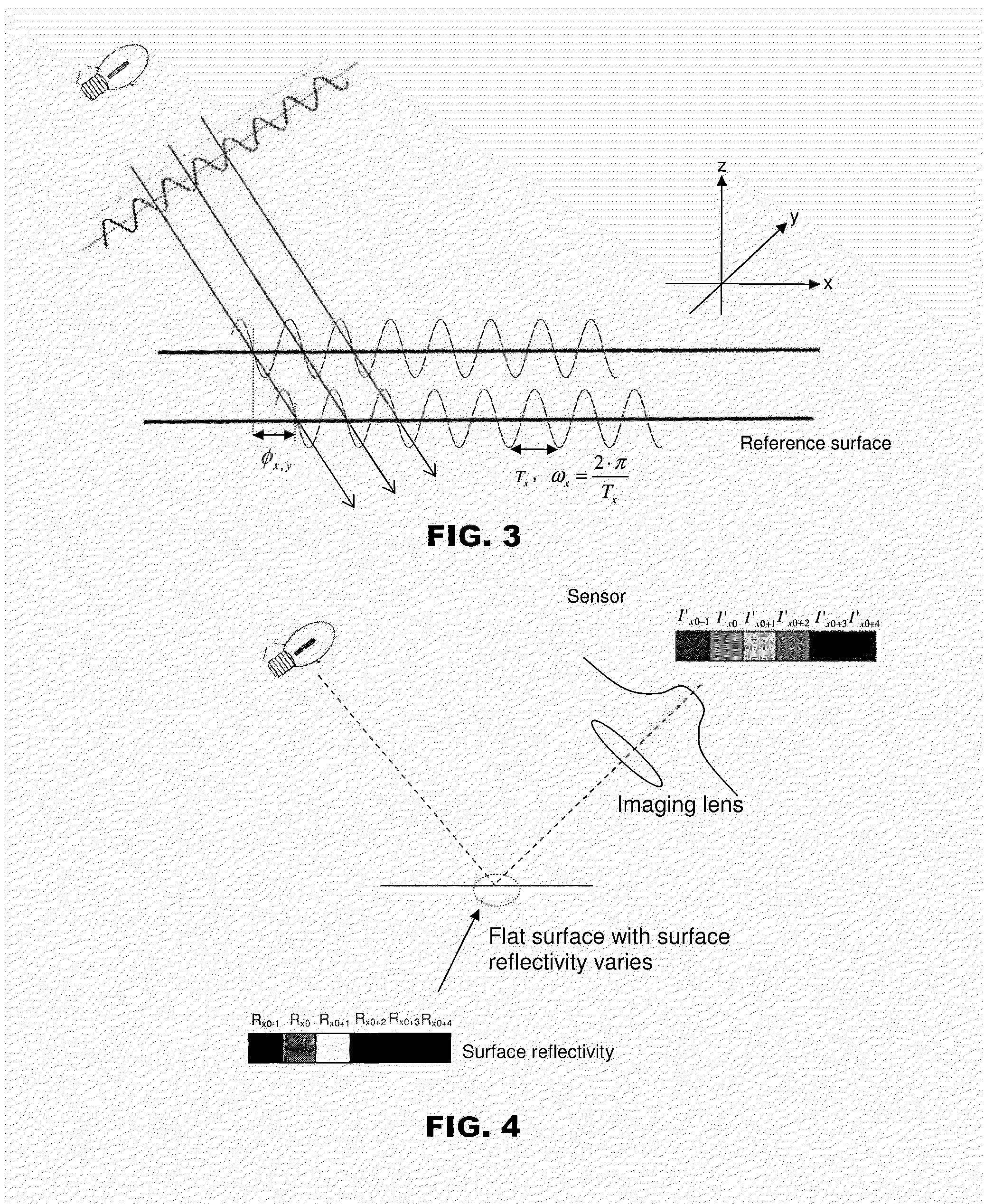
[0021]Light that is emitted from the light source 104 passes through the condenser 106 and illuminates the grating 108. A grating glass comprised in the grating 108 has a series of periodic patterns arranged in a conventional cyclical or sinusoidal pattern which is manufactured with high accuracy as regards their line pitch and linearity. A grating image is formed from the grating 108 and is focused by the lenses 110 onto an object plane level. The device 102 is placed onto the object plane level during ...


PUM


Abstract

An apparatus for inspection of a surface of a device comprises a projection module operative to project a pattern along a projection axis of the projection module onto the device. An imaging module receives an image of the pattern reflected from the device along an imaging axis of the imaging module onto an image sensor. A lens comprised in the imaging module has a first magnification in a first direction orthogonal to the imaging axis and a second magnification different from the first magnification in a second direction orthogonal to both the first direction and the imaging axis, which produces different fields of view of the image sensor and resolutions of the image in the first and second directions.

Description

FIELD OF THE INVENTION[0001]The invention relates to three-dimensional inspection of semiconductor devices, and in particular to three-dimensional measurement of surface profiles of the same employing high resolution pattern projection and imaging.BACKGROUND AND PRIOR ART[0002]The need for automated inspection of semiconductor components and manufactured parts has been growing rapidly in recent decades. A typical method uses a charge-coupled device (“CCD”) to capture two images of the device that is measured. One image provides planar two-dimensional information of the device, and another image provides height information of the device.[0003]One conventional approach for automated three-dimensional inspection is described in U.S. Pat. No. 6,509,559 entitled, “Binary Optical Grating and Method for Generating a Moire Pattern for 3D imaging”. The invention provides a binary grating in a projection system to generate patterned light, and a three-dimensional imaging system images the pat...

Claims


Application Information

Patent Timeline
Patent Type & Authority Applications(United States)
IPC IPC(8): H04N7/18
CPCG01N21/956G01B11/2513
Inventor ZHANG, ZHUANYUNWANG, RAN SHI
Owner ASMPT SINGAPORE PTE LTD
Why Eureka
Try Eureka