Method for producing a BGA chip module and BGA chip module
- Summary
- Abstract
- Description
- Claims
- Application Information
AI Technical Summary
Benefits of technology
Problems solved by technology
Method used
Image

Examples
Embodiment Construction
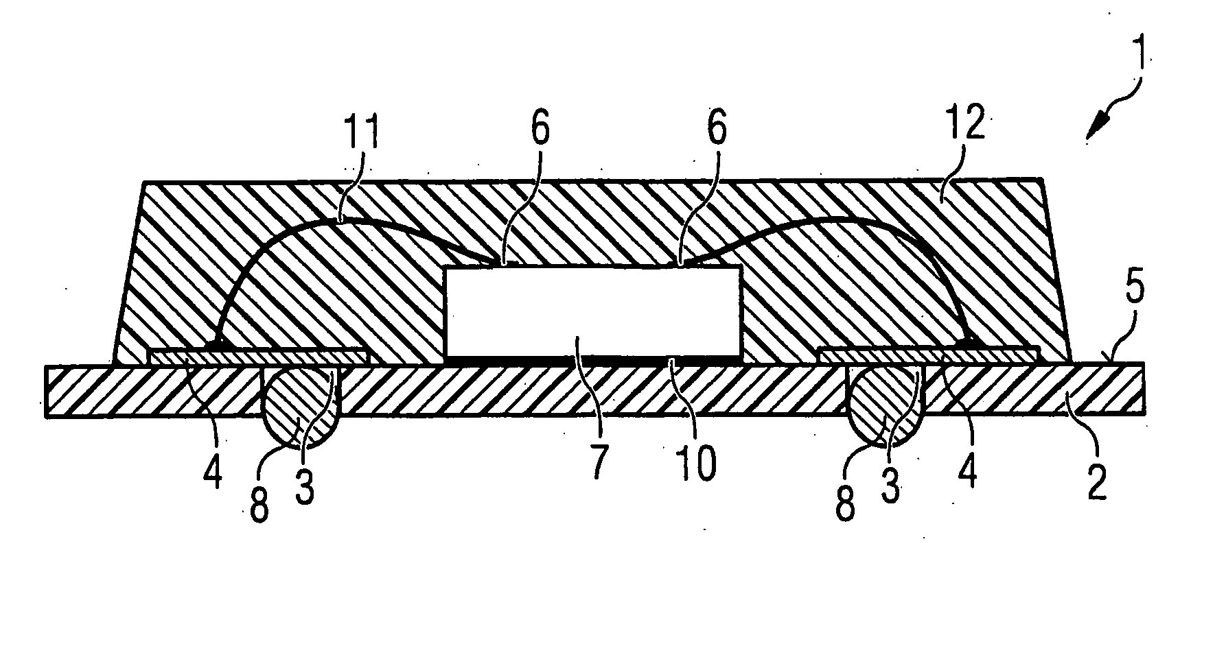
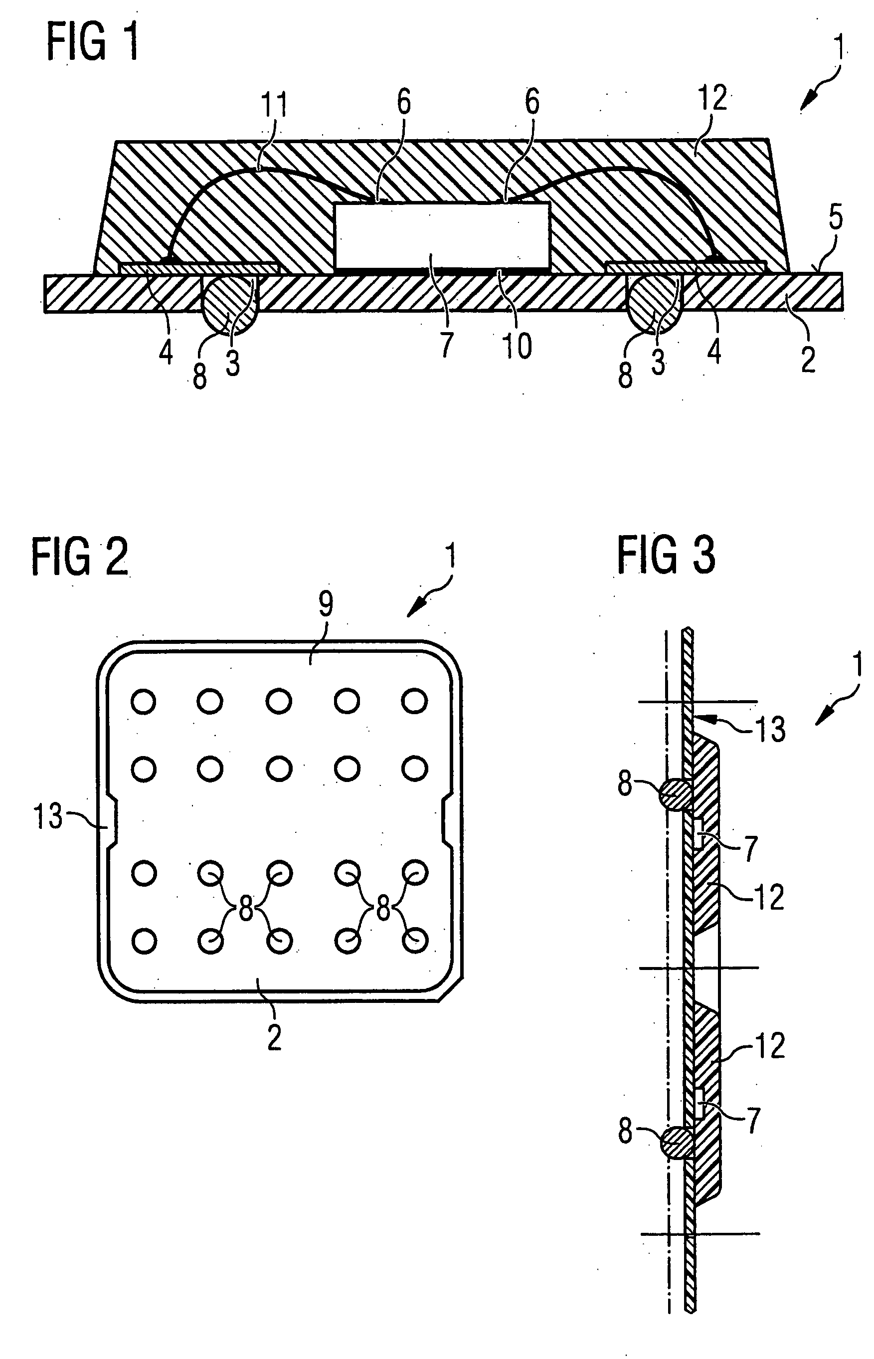
[0013] An advantage of the method according to an exemplary embodiment of the invention is that the forming of holes in a carrier can be implemented very inexpensively, for example by punching. The application of metallization areas is likewise a low-cost production step. The same applies to the introduction of bonding elements into the holes from the underside of the carrier. Consequently, the overall method comprises low-cost production steps using low-cost starting materials. In comparison with the method according to the prior art, it dispenses with the use of expensive multilayered printed circuit boards which have via holes. It likewise dispenses with the method step of applying terminal pads. These are replaced by the bonding elements which are fitted into the holes.
[0014] In an advantageous embodiment, the bonding elements are solder balls. These are of such a size that on the one hand they touch the metallization areas arranged on the upper side of the carrier and on the o...
PUM
 Abstract
Description
Claims
Application Information
 - R&D Engineer
- R&D Manager
- IP Professional
- Industry Leading Data Capabilities
- Powerful AI technology
- Patent DNA Extraction
Browse by: Latest US Patents, China's latest patents, Technical Efficacy Thesaurus, Application Domain, Technology Topic.
© 2024 PatSnap. All rights reserved.Legal|Privacy policy|Modern Slavery Act Transparency Statement|Sitemap