Method and apparatus for synthesizing high-frequency signals for wireless communications

a high-frequency signal and wireless communication technology, applied in the direction of oscillator generators, pulse automatic control, semiconductor/solid-state device details, etc., can solve the problems of critical dependence of the communication system, mixing undesired channels, impure frequency sources creating interference in neighboring channels, etc., to improve manufacturing flexibility, simplify circuitry, and reduce costs

Inactive Publication Date: 2005-11-03
SILICON LAB INC
View PDF1 Cites 19 Cited by
  • Summary
  • Abstract
  • Description
  • Claims
  • Application Information

AI Technical Summary

Benefits of technology

[0014] In accordance with the present invention, a method and apparatus for synthesizing high-frequency signals is disclosed that utilizes on-package oscillator circuit inductors for band selection purposes, thus simplifying circuitry and reducing costs associated with assembly of PLL circuitry. In one embodiment, no external package connection (e.g., package connector pins, package substrate solder bumps, etc.) exists to connect off-package or external inductors (e.g., inductors on printed circuit boards, etc.) to on-package (or within the package) band selection VCO inductance circuits. Advantageously, multiple package electrical connection points may also be provided on-package to allow for selection of alternate oscillator inductance values during package assembly. This increases manufacturing flexibility by allowing manufacture of PLL package circuitry having different hardwired inductance values, using the same package substrate components.
[0015] Oscillator circuit inductors that may be provided on-package using the disclosed method and apparatus include inductors associated with oscillator circuits used to produce output frequencies for mixing with RF and / or IF signals. For example, one or more IF-mixing related inductors of a frequency synthesizer may be provided off-package, while one or more RF-mixing related inductors of the frequency synthesizer may be provided on-package, and vice-versa. Furthermore, as many or as few RF-mixing related and / or IF-mixing related inductors of frequency synthesizer may be provided on-package as desired, advantageously allowing for provision of a frequency synthesizer that may be wholly contained in a single package, including all RF-mixing related and IF-mixing related inductors. As a further advantage, the disclosed on-package frequency synthesizer circuitry may be included with other on-package circuitry, for example, allowing provision of a complete transceiver on-package.
[0019] The disclosed on-package band selection inductance values may be advantageously employed with a variety of different PLL circuitry configurations, for example in one embodiment with a phase-locked loop (PLL) frequency synthesizer having a variable capacitance voltage controlled oscillator (VCO) that includes a discretely variable capacitance in conjunction with a continuously variable capacitance. In such a case, the discretely variable capacitance may provide coarse tuning adjustment of the variable capacitance to compensate for capacitor and inductor tolerances and to adjust the output frequency to be near the desired output frequency. The continuously variable capacitance may provide a fine tuning adjustment of the variable capacitance to focus the output frequency to match precisely the desired output frequency and to provide compensation for post-calibration drift of the PLL circuitry. In such an embodiment, the need for a traditional varactor implementation in the VCO and need for traditional large capacitor component in the loop filter are avoided, thereby providing a high-frequency frequency synthesizer that may be contained in a single package.

Problems solved by technology

The performance of the communication system, however, is critically dependent oh the purity of the synthesized high-frequency output signals.
For signal reception, impure frequency sources result in mixing of undesired channels into the desired channel signal.
For signal transmission, impure frequency sources create interference in neighboring channels.
The level of spectral purity required in cellular telephone applications makes the design of a PLL synthesizer solution and, in particular, the design of a VCO within a PLL synthesizer solution quite demanding.
Phase noise is undesired energy spread continuously in the vicinity of the output frequency, invariably possessing a higher power density at frequencies closer to the fundamental of the output frequency.
Phase noise is often the most damaging of the three to the spectral purity of the output frequency.
It is often the case that the series resistance of the inductor is the dominant loss mechanism in an LC tank oscillator, although other losses typically exist.
The use of off-package or board mounted inductors increases system costs and connection problems may occur at pin connections between the package and a board, adversely affecting reliability and / or performance of the PLL circuitry.

Method used


Image

  • Method and apparatus for synthesizing high-frequency signals for wireless communications
  • Method and apparatus for synthesizing high-frequency signals for wireless communications
  • Method and apparatus for synthesizing high-frequency signals for wireless communications

Examples


Embodiment Construction

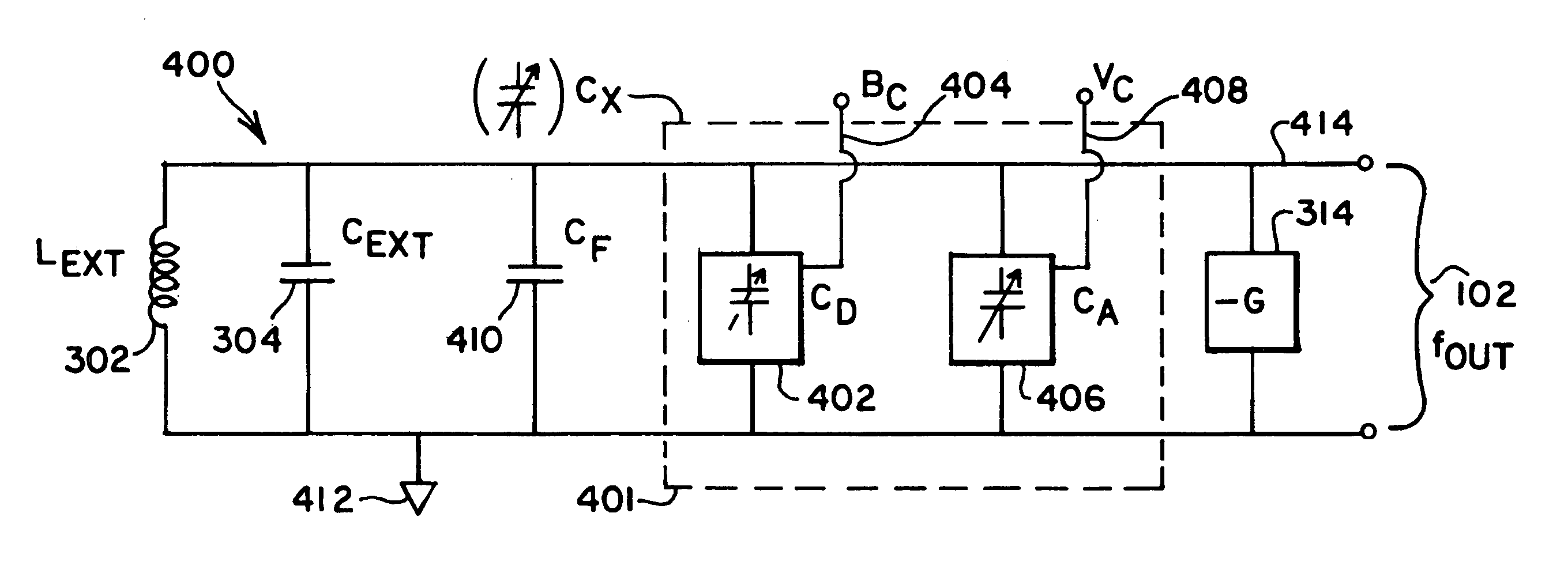
[0054] The present invention contemplates a method and apparatus for synthesizing high-frequency signals by implementing a phase-locked loop (PLL) frequency synthesizer with at least one oscillator circuit having on-package band selection inductor / s. As used herein, “on package” means a particular component is mounted or otherwise disposed within or on a semiconductor package that includes an integrated circuit die mounted or otherwise structurally contained within the package. In this regard, an integrated circuit may be electrically connected within the package to a lead frame or other package substrate suitable for electrically connecting the integrated circuit to external package connectors including, but not limited to, pin connectors, lead connectors, solder bumps, etc. “Off package” means that a particular component is not mounted or otherwise disposed within such a semiconductor package, but rather is mounted or disposed separate from the package (e.g., on a printed circuit ...


PUM


Abstract

A semiconductor package includes a package substrate and an integrated circuit. The package substrate has a first surface. The integrated circuit couples electrically to the first surface of the package substrate. The integrated circuit and the package substrate together form the semiconductor package. The semiconductor package also includes a first inductance circuit and a second inductance circuit, both formed within the semiconductor package. The first and second inductance circuits couple to each other in parallel. The first and second inductance circuits have substantially symmetrical geometric characteristics.

Description

CROSS-REFERENCE TO RELATED PATENT DOCUMENTS [0001] This patent application is a continuation-in-part application of U.S. patent application Ser. No. 09 / 999,702, Attorney Docket No. SILA:060C1, titled “Method and Apparatus for Synthesizing Dual Band High-Frequency Signals for Wireless Communications,” filed on Oct. 31, 2001, which is a continuation application of U.S. patent application Ser. No. 09 / 579,151, Attorney Docket No. SILA:060, titled “Method and Apparatus for Synthesizing Dual Band High-Frequency Signals for Wireless Communications,” filed on May 25, 2000, now issued as U.S. Pat. No. 6,323,735. [0002] This patent application claims priority to, and incorporates by reference, the following patent documents: U.S. patent application Ser. No. ______, Attorney Docket No. SILA:074, titled “Radio-Frequency Communication Apparatus and Associated Methods”; U.S. patent application Ser. No. ______, Attorney Docket No. SILA:075, titled “Apparatus and Methods for Generating Radio Freque...

Claims


Application Information

Patent Timeline
Patent Type & Authority Applications(United States)
IPC IPC(8): H01L23/66H03B5/00H03L7/099H03L7/10H03L7/18H03L7/199
CPCH01L23/66H01L24/49H01L2224/48227H01L2224/16225H01L2924/014H01L2924/01033H01L24/48H03L7/199H03L7/18H01L2223/6611H01L2224/16H01L2224/48091H01L2224/48247H01L2224/49113H01L2224/49171H01L2924/01006H01L2924/01015H01L2924/0102H01L2924/01046H01L2924/01082H01L2924/14H01L2924/15192H01L2924/15311H01L2924/19041H01L2924/19042H01L2924/30105H01L2924/30107H03L7/099H03L7/10H01L2924/00014H01L2924/00H01L2224/05554H01L2924/15787H01L2924/181H03L7/104H01L2224/45099H01L2224/05599H01L2924/00012H01L2224/0401
Inventor LIM, LYSANDERWELLAND, DAVID R.PAVELKA, JOHN B.HEALY, EDMUND G.
Owner SILICON LAB INC
Why Eureka
Try Eureka