Liquid crystal electro-optic device

a liquid crystal electrooptic and electrooptic technology, applied in optics, instruments, transistors, etc., can solve the problems of large difference in the horizontal direction of electrode thickness between the top and the base of the electrode, non-continuous electric inability to ignore the problem of large non-continuous electric field at the electrode vertices, etc., to achieve the effect of improving the display characteristics of the device, non-continuous electric field strength around the pixel

Inactive Publication Date: 2005-11-03
SEMICON ENERGY LAB CO LTD
View PDF40 Cites 4 Cited by
  • Summary
  • Abstract
  • Description
  • Claims
  • Application Information

AI Technical Summary

Benefits of technology

[0022] It is therefore an object of the invention to provide a liquid crystal electro-optic device which has an electrode structure such that noncontinuity of the electric field strength around each pixel electrode is minimized and the display characteristics of the device are thereby improved and which can be made by a simple method.

Problems solved by technology

However, electrodes of the super TFT method conventionally used have been of a trapezoidal or rectangular structure, and the electric fields produced by these electrodes have been noncontinuous at vertices of the trapezoid or rectangle.
This kind of noncontinuity of the electric field at the electrode vertices is a problem which cannot be ignored when making very small pixels.
However, in making extremely tall electrodes, the following technological difficulties arise.
Firstly, when the height of an electrode is made as great as the cell thickness, a large difference in the horizontal direction electrode thickness tends to arise between the top and the base of the electrode.
Consequently, because the electric field strength in the cell thickness direction varies within the same pixel, driving the liquid crystal becomes difficult.
Secondly, when the electrodes are extremely tall, the coverage of layers formed on top of the electrodes is poor and line breakage tends to occur.
Thirdly, in making very small pixels, with extremely tall electrodes it is difficult to make the horizontal direction film thickness thin and obtain a large taper angle.

Method used


Image

  • Liquid crystal electro-optic device
  • Liquid crystal electro-optic device
  • Liquid crystal electro-optic device

Examples


Embodiment Construction

[0079] Preferred embodiments of the invention will now be described.

[0080] (First Preferred Embodiment)

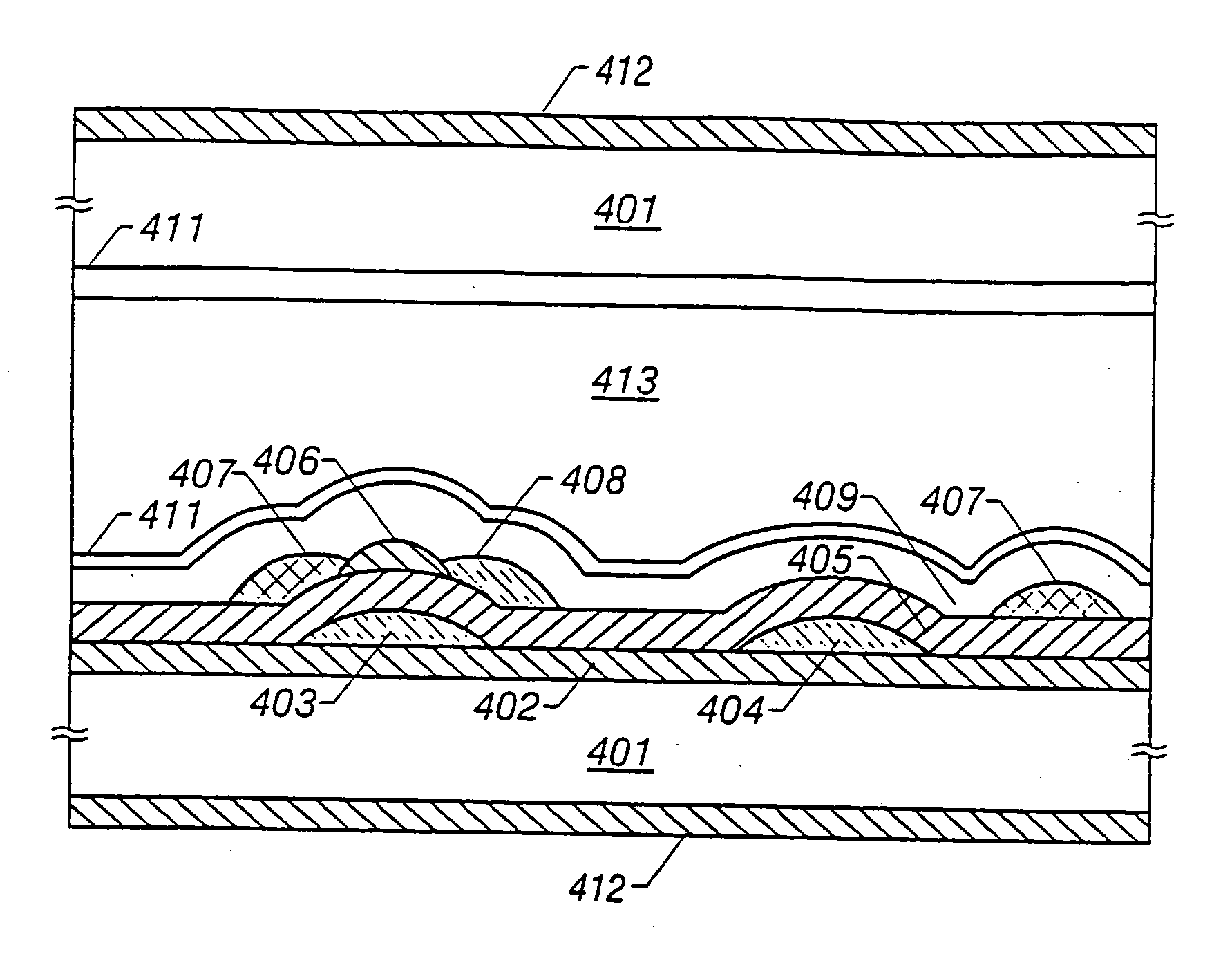
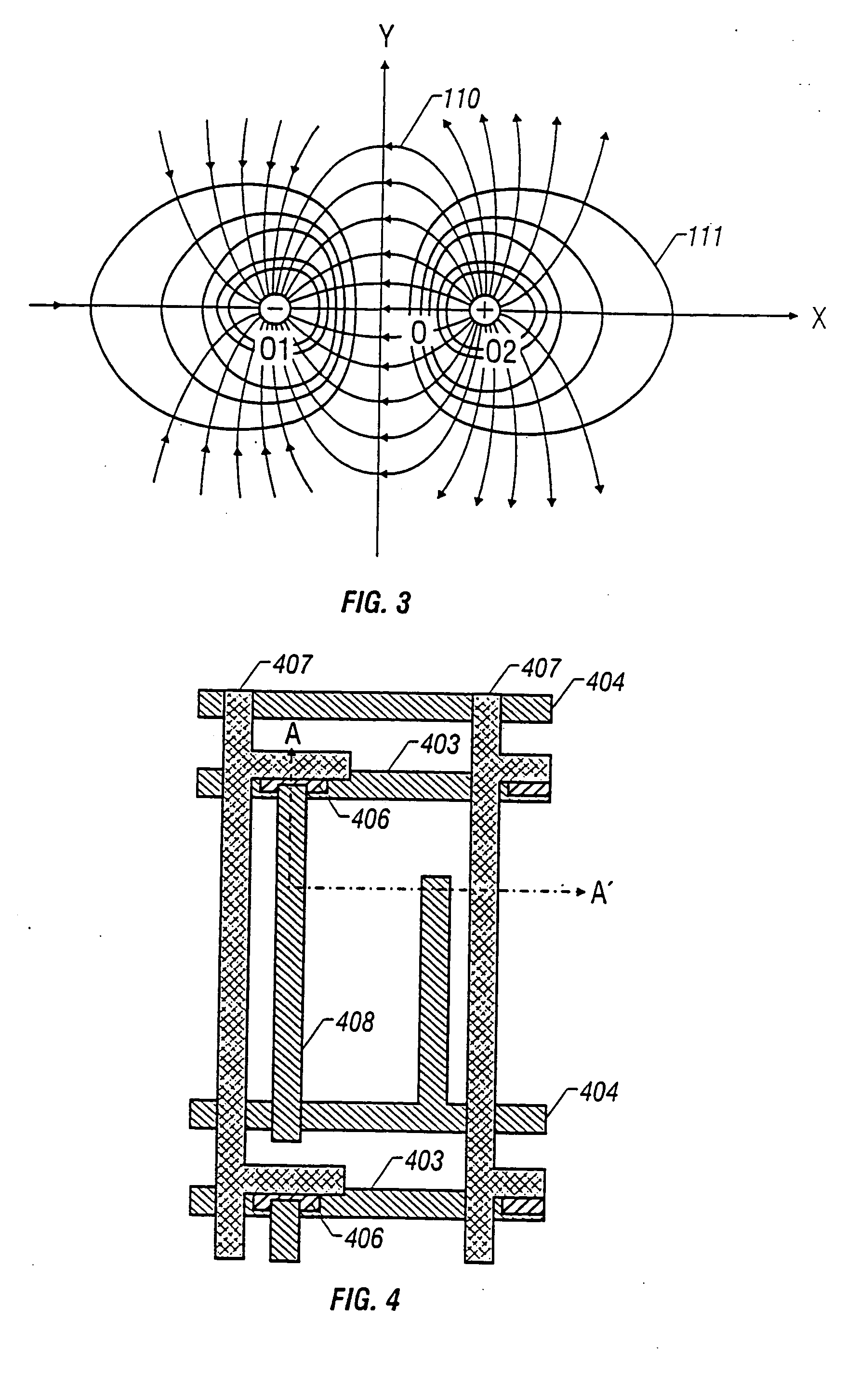
[0081] A silicon oxide film of thickness 1000 to 3000 Å was formed as a base oxide film (402) on a Corning #7059 insulating substrate (401). As the method of forming this silicon oxide film, sputtering in an oxygen atmosphere or plasma CVD can be used. A film of Cr was then formed on this to a thickness of 1000 to 5000 Å and patterned. After that, isotropic plasma etching was carried out using resist as a mask. At this time, the discharge gas voltage was suitably set to give the electrodes curved surfaces. In this way, a gate electrode (403) and a common electrode (404) were formed.

[0082] A gate insulating film (405) consisting of silicon dioxide (SiO2) was then formed so as to cover these electrodes. This film may alternatively consist of silicon nitride (SiN). An amorphous silicon film (406) was then formed on the gate insulating film above the gate electrode. Then, a source e...


PUM

PropertyMeasurementUnit
temperatureaaaaaaaaaa
insulatingaaaaaaaaaa

Abstract

In a horizontal electric field drive type liquid crystal electro-optic device wherein a liquid crystal material is driven by controlling the strength of an electric field parallel to a substrate, noncontinuity of the electric field strength around each pixel electrode is minimized and thereby the occurrence of flaws in the orientation of the liquid crystal material and dispersion in operation are reduced and a construction having improved display characteristics and a method of manufacturing the same are provided. In a horizontal electric field drive type liquid crystal electro-optic device wherein a gate electrode 403, a source electrode 407, a drain electrode 408, a semiconductor film 406 and a common electrode 404 are formed on a glass substrate and a liquid crystal material is driven by controlling the strength of an electric field substantially parallel to the glass substrate, the electrodes and the semiconductor film are made curved, for example semi-circular or semi-elliptical, in sectional profile. These curved sectional profiles can be formed by suitably selecting and combining various patterning and etching methods.

Description

BACKGROUND OF THE INVENTION [0001] This invention relates to a liquid crystal electro-optic device having good electrical characteristics and angle of visibility characteristics with which a uniform display can be obtained over an entire screen. [0002] As a method of widening the angle of visibility of a liquid crystal electro-optic device, a method wherein the direction of an electric field impressed on a liquid crystal is made substantially parallel to the surface of a substrate (hereinafter referred to as the super TFT method) is disclosed for example in Japanese Unexamined Patent Publication No. H.6-160878. In this case, an electric field is induced between a source electrode and a common electrode formed on one substrate, and the liquid crystal molecules are oriented in the direction of this electric field. Also, in Japanese Unexamined Patent Publication No. H.6-214244, the electric field impressed on the liquid crystal is made uniform by making the height of the electrodes the...

Claims


Application Information

Patent Timeline
Patent Type & Authority Applications(United States)
IPC IPC(8): G02F1/1343G02F1/136G02F1/1368H01L29/786
CPCG02F1/1368G02F1/134363G02F1/134336G02F1/136G02F1/1343
Inventor YAMAZAKI, SHUNPEINISHI, TAKESHISATAKE, RUMO
Owner SEMICON ENERGY LAB CO LTD
Why Eureka
Try Eureka