Liquid crystal display and method of manufacturing the same

a technology of liquid crystal display and liquid crystal, which is applied in the manufacture of electric discharge tubes/lamps, basic electric elements, instruments, etc., can solve the problems of considerable thickness of the polarizer attached to the outside of the display panel, and achieve the effect of improving the display characteristic and decreasing light refraction

Inactive Publication Date: 2010-08-12
SAMSUNG ELECTRONICS CO LTD
View PDF20 Cites 42 Cited by
  • Summary
  • Abstract
  • Description
  • Claims
  • Application Information

AI Technical Summary

Benefits of technology

[0008]Exemplary embodiments of a liquid crystal display capable of improving the display characteristic by decreasing light refraction, and a method of manufacturing the same will be described.

Problems solved by technology

However, the polarizer attached to the outside of display panel has a considerable thickness, so the polarizer may partially refract incident light on the display panel or light emitted from the display panel.

Method used


Image

  • Liquid crystal display and method of manufacturing the same
  • Liquid crystal display and method of manufacturing the same
  • Liquid crystal display and method of manufacturing the same

Examples


example 1

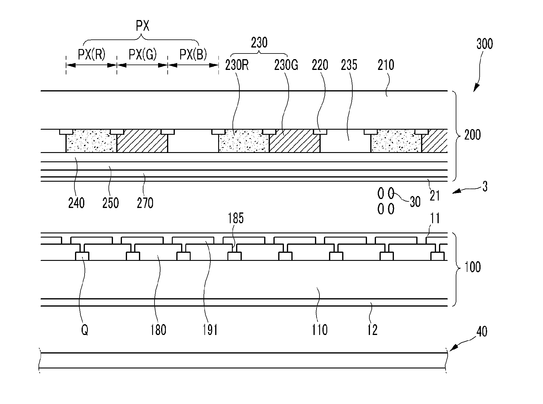
[0102]A negative photosensitive layer is formed on a glass substrate at a thickness of about 2 micrometers (μm) to about 4 μm, and exposed with light of a wavelength region of about 350 nm to about 440 nm by using a mask including a predetermined pattern. The exposed negative photosensitive layer formed on the glass substrate is subjected to a post-exposure baking process at a temperature of about 110° C. for about 90 seconds. The photosensitive layer is developed in a 2.38% TMAH solution to provide a black matrix.

[0103]A red phosphor solution containing Y2O2S:Eu and a green phosphor solution containing BaMgAl10O17:Eu,Mn are individually prepared. The red phosphor solution is coated on a surface of a rubber stamp, and the solvent is evaporated. The rubber stamp is printed on the substrate to provide a red phosphor. Subsequently, the green phosphor solution is coated on a surface of another rubber stamp, the solvent is evaporated, and the resulting green phosphor solution is printed ...

example 2

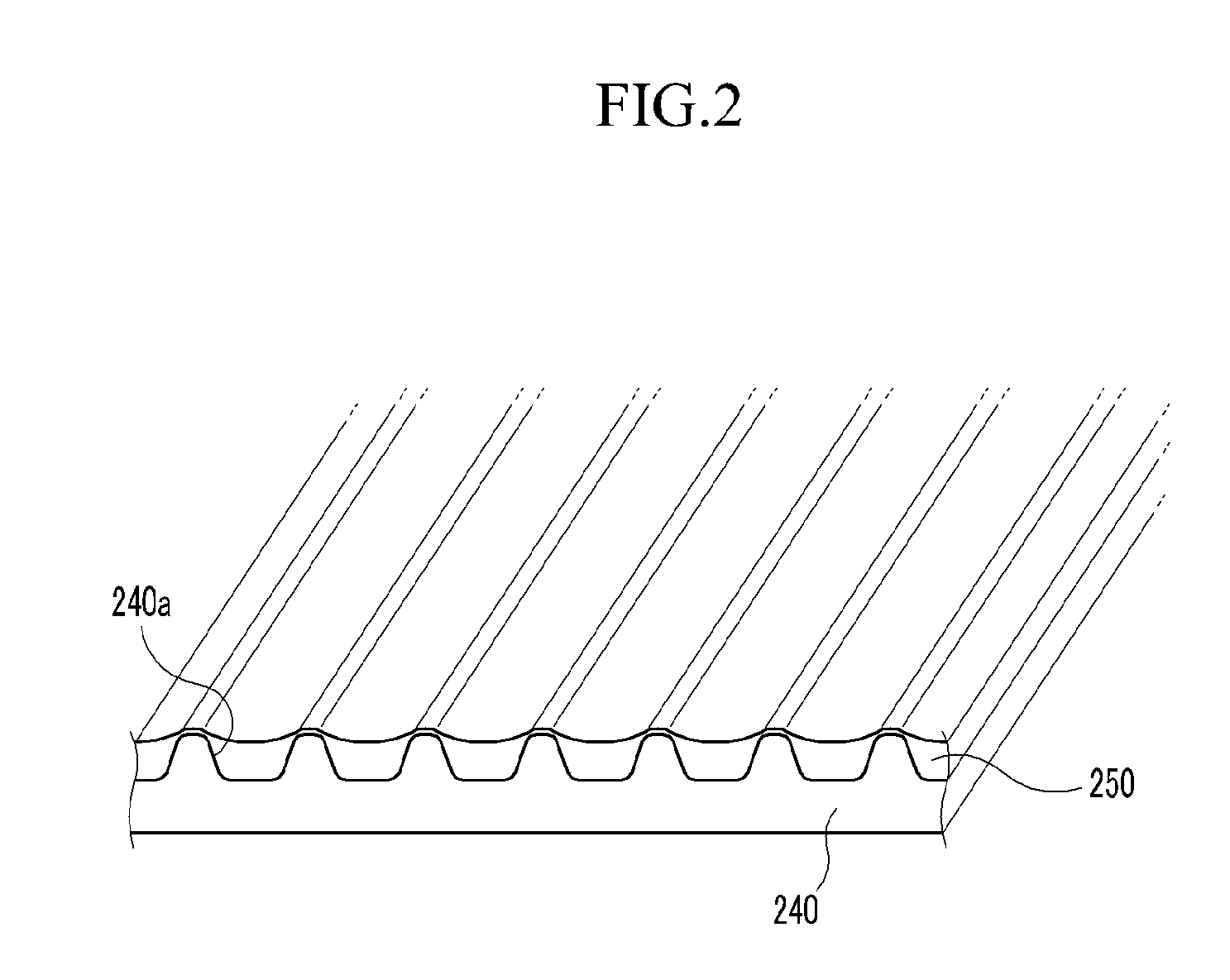
[0107]The next exemplary embodiment is carried out in accordance with the same procedure as in Example 1, except that the insulator is prepared by diluting SE7492K (manufactured by Nissan Chemical Korea Co. Ltd.) forming about 6% of polyimide in a N-methylpyrrolidone solvent, spin-coating at about 3000 revolutions per minute (rpm) for about 30 seconds, allowing the same to stand at about 300° C. for about 1 hour, and cooling and rubbing the same.

example 3

[0108]The next exemplary embodiment is carried out in accordance with the same procedure as in Example 2, except that the insulator is prepared by spin-coating PI-B (manufactured by Nissan Chemical Co. Ltd.), prebaking the same at about 80° C. for about 15 minutes, allowing the same to stand at about 250° C. for about 1 hour, and cooling the same.


PUM

PropertyMeasurementUnit
thicknessaaaaaaaaaa
sizeaaaaaaaaaa
thicknessaaaaaaaaaa

Abstract

Disclosed is a liquid crystal display which includes a first display panel including a plurality of pixel electrodes, a second display panel facing the first display panel, and a liquid crystal layer interposed between the first display panel and the second display panel, and a method of manufacturing the liquid crystal display panel. The second display panel includes a light emitting element displaying a color, an insulating layer disposed on the light emitting element and including a rubbed surface, a polarization layer disposed on the insulating layer and opposite to the light emitting element with respect to the insulating layer, and a common electrode disposed on the polarization layer and facing the pixel electrode.

Description

CROSS-REFERENCE TO RELATED APPLICATION[0001]This application claims priority to Korean Patent Application No. 10-2009-0009918 filed on Feb. 6, 2009, and all the benefits accruing therefrom under 35 U.S.C. §119, the entire contents of which are incorporated herein by reference.BACKGROUND[0002]1. Field[0003]This disclosure relates to a liquid crystal display (“LCD”) and a method of manufacturing the same.[0004]2. Description of the Related Art[0005]A liquid crystal display is a flat panel display which is being widely used. The liquid crystal display includes two display panels provided with field generating electrodes and a liquid crystal layer interposed therebetween. Liquid crystal molecules in the liquid crystal layer are rotated depending upon an electric field formed between the field generating electrodes to thereby vary light transmittance to display images.[0006]The liquid crystal display includes a polarizer attached to the outside of the display panel. The polarizer selecti...

Claims


Application Information

Patent Timeline
Patent Type & Authority Applications(United States)
IPC IPC(8): G02F1/1335H01J9/24
CPCG02F1/133528G02F1/133617G02F2202/36G02F2001/133548G02F2001/133565G02F2001/01791G02F1/01791G02F1/133548G02F1/133565G02B5/28
Inventor JUNG, WON-CHEOLKIM, BYUNG-KIIM, SEOUNG-JAE
Owner SAMSUNG ELECTRONICS CO LTD
Why Eureka
Try Eureka