Electro-optic device, method for manufacturing electro-optic device, projector, and electronic apparatus

a manufacturing method and electrooptic technology, applied in the field of electrooptic devices, can solve the problems of reducing light utilization efficiency, increasing the cost of attaching the cover glass, and deformation or breakage of the light shielding portion, and achieves high display characteristics, high contrast, and bright display

Inactive Publication Date: 2007-08-30
SEIKO EPSON CORP
View PDF15 Cites 40 Cited by
  • Summary
  • Abstract
  • Description
  • Claims
  • Application Information

AI Technical Summary

Benefits of technology

[0037]In accordance with a further embodiment of the invention, an electronic apparatus includes a low-cost thin electro-optic device capable of a bright display, and thus it may be possible to provide an electronic apparatus including a high-quality display portion having high contrast and high display characteristics.

Problems solved by technology

When the groove is formed in the substrate surface, the light-shielding portion may be deformed or broken due to sinking in the groove.
In addition, in the configuration shown in FIG. 5 of Japanese Unexamined Patent Application Publication No. 3-170911, reflected light is transmitted through the cover glass and is applied to the light-shielding portion, thereby decreasing the light utilization efficiency.
Furthermore, the cost is increased by attaching the cover glass.
When the thermal expansion coefficients of the filler and the substrate greatly differ from each other, the substrate may be deformed to hinder the function of each functional element provided on the electro-optic device.

Method used


Image

  • Electro-optic device, method for manufacturing electro-optic device, projector, and electronic apparatus
  • Electro-optic device, method for manufacturing electro-optic device, projector, and electronic apparatus
  • Electro-optic device, method for manufacturing electro-optic device, projector, and electronic apparatus

Examples


first embodiment

(Projector)

[0072]First, the schematic configuration of a projector according to a first embodiment of the invention will be described.

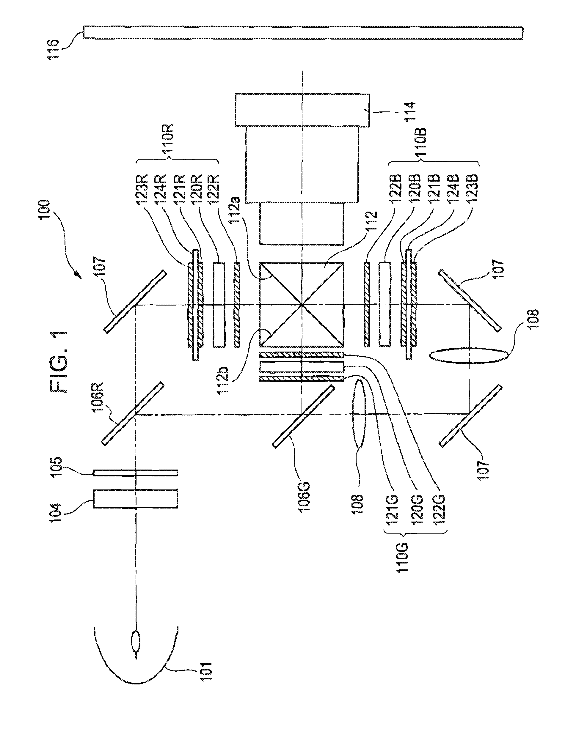
[0073]As shown in FIG. 1 an extra-high pressure mercury lamp 101 serving as a light source supplies light containing red light (referred to as “R light” hereinafter) as first color light, green light (referred to as “G light” hereinafter) as second color light, and blue light (referred to as “B light” hereinafter) as third color light. An integrator 104 makes uniform an illumination distribution of light supplied from the extra-high pressure mercury lamp 101. The light with a uniform illumination distribution is converted to polarized light having a specified vibration direction, for example, s-polarized light, by a polarization conversion element 105. The s-polarized light is incident on a R light transmitting dichroic mirror 106R constituting a color separation optical system. The R light will be described below. The R light transmitting dichroic mi...

second embodiment

[0131]Next, a second embodiment of the invention will be described. This embodiment is different from the first embodiment in material and composition of a filler formed in grooves of prism elements and manufacturing method. Therefore, these points are mainly described.

(Prism Element)

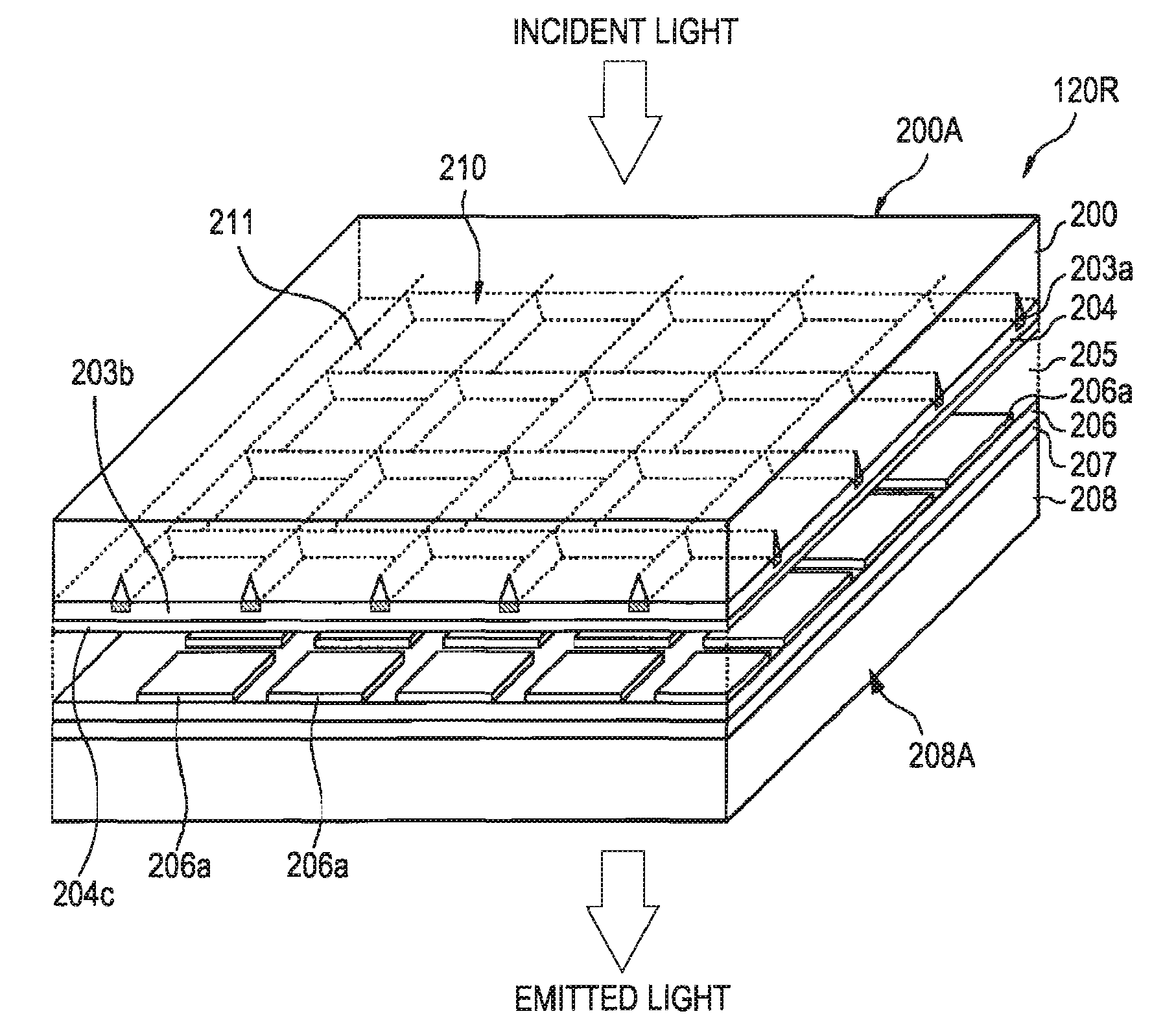
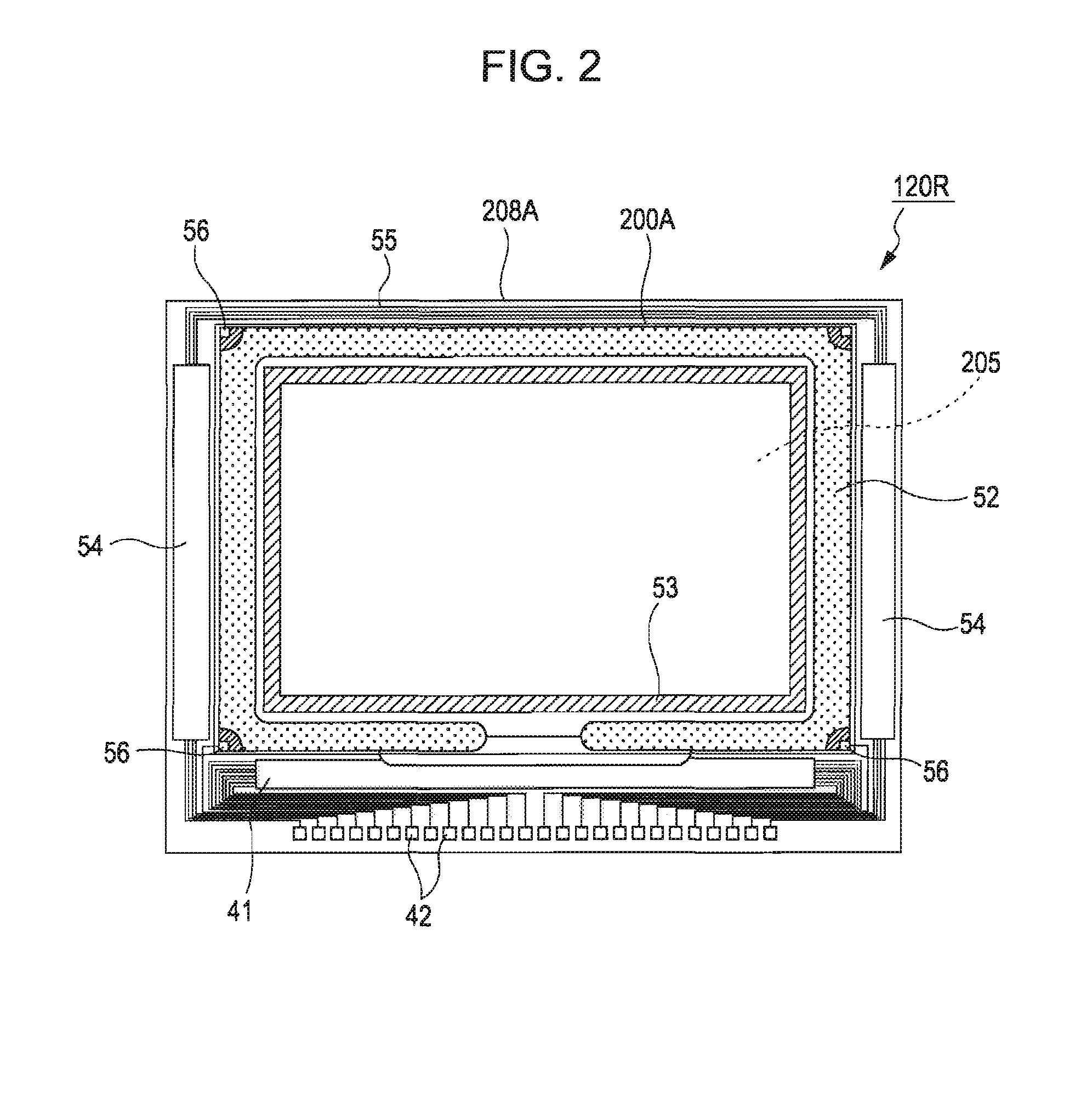
[0132]FIG. 12 is a sectional view showing the configuration of a liquid crystal panel 320R.

[0133]Each of prism elements 311 serves as an optical path deflecting portion having a groove 363 formed to extend inward from the inner surface of a counter substrate 300. The groove 63 is provided with a filter 312 composed of an inorganic material such as sol-gel glass or silicon as a raw material. The prism elements 311 have an isosceles triangular section. A filler 312 composed of an inorganic material such as sol-gel glass or silicon as a raw material is formed in the grooves 363. The filler 312 is formed in the grooves 363 of the prism elements 311 so as to cover the inner surface of the counter substrate 3...

third embodiment

[0142]A third embodiment of the invention will be described. This embodiment is different from the first embodiment in configuration of a filler formed in grooves of prism elements and a light-shielding portion, and thus this point is mainly described.

[0143]FIG. 16 is a sectional view showing the configuration of a liquid crystal panel 420R.

[0144]Each of prism elements 411 serves as an optical path deflecting portion having a groove 463 formed to extend inward from the inner surface of a counter substrate 400. Like in the first embodiment, the groove 463 is provided with a filter 412 composed of, for example, an acrylic resin as a raw material. The prism elements 411 have an isosceles triangular section. The filler 412 is formed to fill in the grooves 463 of the prism elements 411 so that the surface 412a of the filler 412 is positioned deeper than the inner surface of the counter substrate 400.

[0145]A light-shield portion 403a is formed on the surface 412a of the filler 412 to fill...


PUM

PropertyMeasurementUnit
angleaaaaaaaaaa
refractive indexaaaaaaaaaa
thermal expansion coefficientaaaaaaaaaa

Abstract

An electro-optic device includes a pair of substrates, and an electro-optic material held between the pair of substrates, wherein one of the pair of substrates includes a condensing unit provided on the electro-optic material-side surface of the substrate in order to condense light incident on the substrate, and a functional layer provided to overlap at least the condensing unit in a plan view.

Description

BACKGROUND[0001]1. Technical Field[0002]Several aspects of the present invention relates to an electro-optic device, a method for manufacturing an electro-optic device, a projector, and an electronic apparatus.[0003]2. Related Art[0004]An image display area of an electro-optic device used as a light valve of a projector includes a pixel region which emits light and a pixel-to-pixel region in which wiring is formed for supplying electric signals to the pixel region. For example, in a liquid crystal device, the pixel-to-pixel region is generally covered with a light-shielding portion to prevent transmission of light in this region.[0005]In such an electro-optic device, preferably, the quantity of light emitted from the pixel region is as large as possible and the emitted light is bright light, and it is desired to realize high light utilization efficiency. For example, Japanese Unexamined Patent Application Publication No. 3-170911 discloses a liquid crystal device using an optical el...

Claims


Application Information

Patent Timeline
Patent Type & Authority Applications(United States)
IPC IPC(8): G02F1/1335
CPCG02F1/1303G02F1/133512G02F1/133553H04N9/3197G02F2001/133607H04N9/3105G02F2001/133565G02F1/133565G02F1/133607G03B21/00G03B21/14H04N9/31
Inventor KAMIJIMA, SHUNJI
Owner SEIKO EPSON CORP
Why Eureka
Try Eureka