Electro-optical device and electronic apparatus

a technology of optical devices and electronic devices, applied in non-linear optics, instruments, optics, etc., can solve the problems of easy generation of diffraction light, increased size of spread of light emitted from liquid crystal devices, and portion of light being subjected to vignetting by projection lenses, etc., to reduce the influence of diffraction light, easy manufacturing, and excellent cost competitiveness

Inactive Publication Date: 2015-02-12
SEIKO EPSON CORP
View PDF5 Cites 35 Cited by
  • Summary
  • Abstract
  • Description
  • Claims
  • Application Information

AI Technical Summary

Benefits of technology

[0011]According to the configuration of this application example, the lens diameters of the first micro lenses which correspond to the first pixels differ from the lens diameters of the second micro lenses which correspond to the second pixels, which are adjacent to the first pixels. In other words, two micro lenses with different lens diameters are arranged to be adjacent to one another. Therefore, when, as in the related art, the micro lenses with the same lens diameters are arranged, the repeating pattern is per-pixel; conversely, the configuration of this application example is capable of doubling the repetition period, since the repeating pattern is provided for every two pixels. Accordingly, in comparison to a case in which, as in the related art, the micro lenses with the same lens diameters are arranged, it is possible to suppress the spread angle of the light caused by the interference of diffracted light arising from the micro lenses. It is possible to form the first micro lenses and the second micro lenses, in which the lens diameters are alternately different, in the same process by performing an etching process or the like using masks in which the opening diameters of the opening portions are different, for example. Accordingly, it is possible to provide the liquid crystal device which can reduce the influence of the diffraction of light, and which includes the micro lens array that can be manufactured easily.Application Example 2
[0015]According to the configuration of this application example, since the m×n micro lenses in which the lens diameters are alternately different are arranged to repeat as units, by increasing the number of at least one of m and n, it is possible to further increase the repetition period of the micro lenses with different lens diameters. Accordingly, it is possible to further reduce the influence of the diffraction of the light.Application Example 4
[0017]According to the configuration of this application example, the m×n micro lenses which are arranged repeatedly in the first row and the m×n micro lenses which are arranged repeatedly in the second row which is adjacent to the first row are disposed to be shifted alternately in the first direction. Therefore, it is possible to further increase the repetition period of the micro lenses with different lens diameters in comparison to a case in which the m×n micro lenses are not disposed to be shifted when comparing the first row and the second row. Accordingly, it is possible to more effectively reduce the influence of the diffraction of the light.Application Example 5
[0019]According to the configuration of the application example, since both the first substrate and the second substrate are provided with the plurality of micro lenses, it is possible to suppress the spreading of the light which is emitted from the electro-optical device by restoring the angle of the condensed light using the micro lenses of the substrate of the emission side in addition to improving the efficiency for light utilization by condensing the light using the micro lenses of the substrate of the incidence side. Since the m×n micro lenses are disposed to be shifted alternately in at least one direction when comparing the first substrate and the second substrate, in comparison to a case in which the m×n micro lenses are not shifted alternately, it is possible to further suppress the spread angle of the light caused by the interference of diffracted light arising from the micro lenses.Application Example 6
[0021]According to the configuration of this application example, it is possible to provide an electronic apparatus with a bright display and excellent cost competitiveness, since the electronic apparatus is provided with the electro-optical device which can effectively reduce the influence of the diffraction of light, and which includes the micro lens array that can be manufactured easily.

Problems solved by technology

Incidentally, in the liquid crystal device provided with the micro lens array, since the micro lenses are arranged in an orderly (periodic) manner corresponding to the arrangement pitch of the pixels, the incident light is diffracted, diffracted light is easily generated, and the spread of the light which is emitted from the liquid crystal device may increase in size due to the diffracted light interfering with itself.
When using the liquid crystal device provided with such a micro lens array as a liquid crystal light bulb of a projector, when the spread angle of the light emitted from the liquid crystal device is equal to or greater than the F number of the projection lens, there is a problem in that a portion of the light is subjected to vignetting by the projection lens and the image which is shown on a screen becomes dark.
However, JP-A-2005-352392 does not disclose a method of forming the micro lens array of the above-described configuration.
Forming a plurality of micro lenses with the same planar shape and different radii of curvature in the same process by performing an isotropic etching process using a general mask is considered to be difficult.
Even when the refractive index differences between the micro lenses and the adjacent member are caused to differ, the manufacturing process becomes complex due to using materials with different refractive index for each micro lens.
Furthermore, when the liquid crystal device provided with a micro lens array in which the shape of curvature or the refractive index difference is caused to differ for each micro lens is used as a liquid crystal light bulb, there is a concern that the image displayed on the screen will become dark.

Method used


Image

  • Electro-optical device and electronic apparatus
  • Electro-optical device and electronic apparatus
  • Electro-optical device and electronic apparatus

Examples


first embodiment

Electro-Optical Device

[0042]Here, description is given exemplifying an active matrix liquid crystal device, which is provided with a Thin Film Transistor (TFT) as a pixel switching element, as the electro-optical device. For example, the liquid crystal device can be favorably used as a light modulating element (a liquid crystal light bulb) of a projection-type display device (a projector) described later.

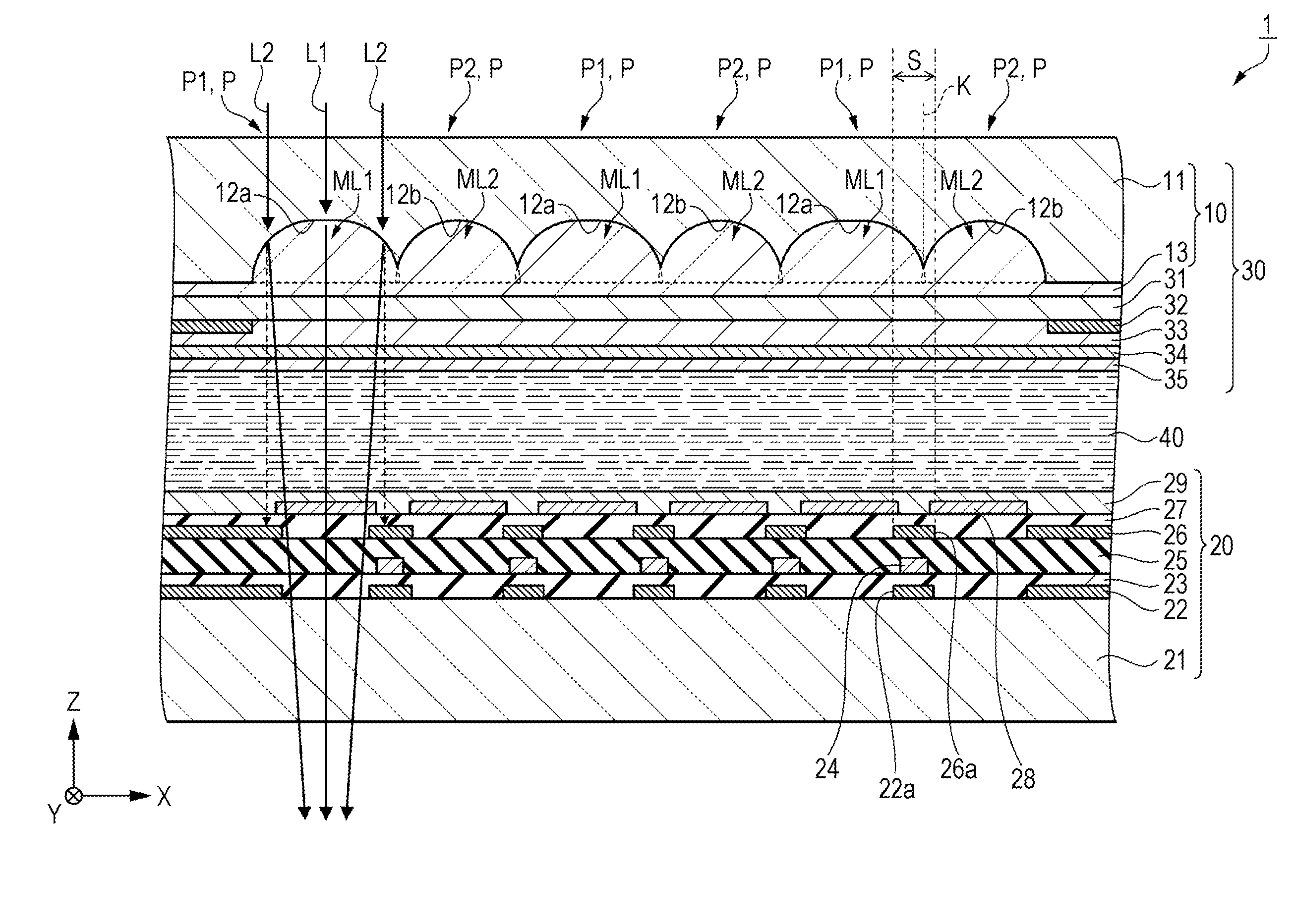
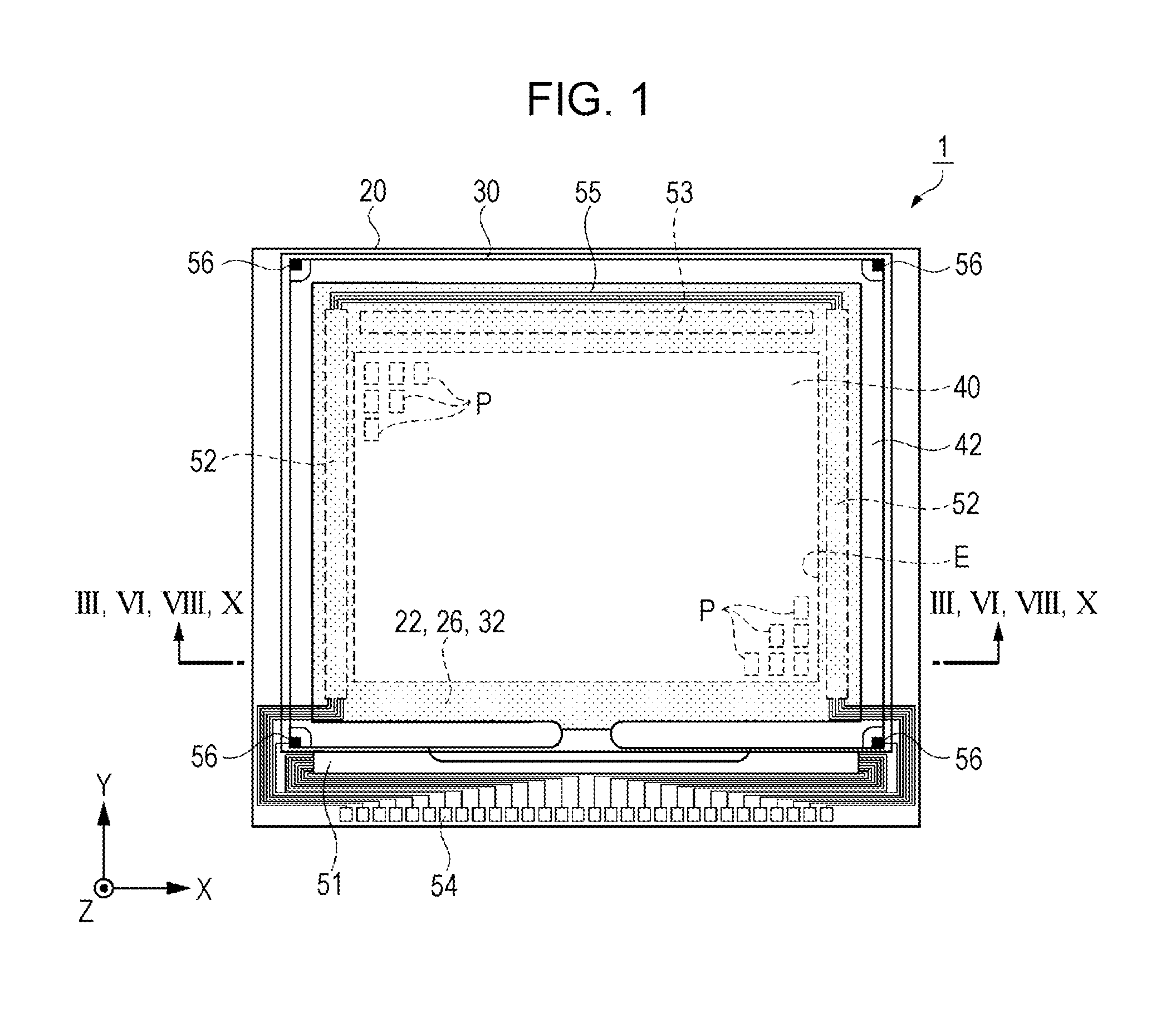
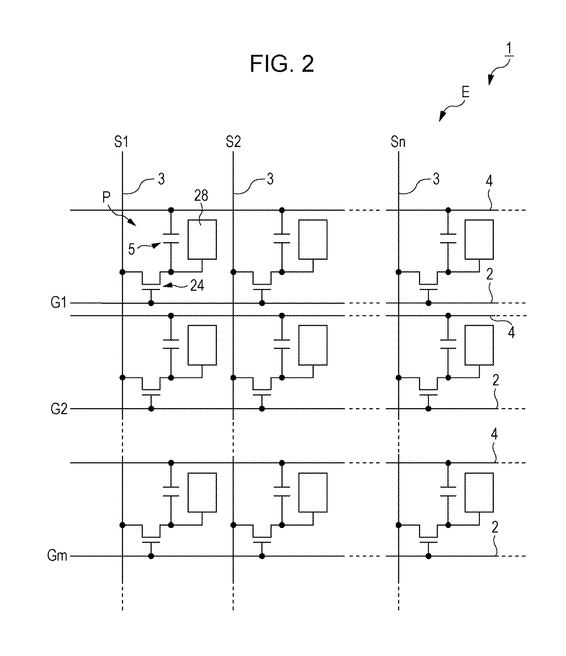
[0043]First, description will be given of the liquid crystal device as the electro-optical device according to the first embodiment, with reference to FIGS. 1 to 3. FIG. 1 is a schematic plan view showing the configuration of the liquid crystal device according to the first embodiment. FIG. 2 is an equivalent circuit diagram showing the electrical configuration of the liquid crystal device according to the first embodiment. FIG. 3 is a schematic cross-sectional diagram showing a configuration of the liquid crystal device according to the first embodiment. Specifically, FIG. 3 is a s...

second embodiment

[0111]A liquid crystal device according to the second embodiment has a configuration that is substantially the same as that of the first embodiment except in that the configuration of the micro lens array substrate is different. Here, description will be given mainly of the differences in the configuration and the manufacturing method of the micro lens array substrate in relation to the first embodiment. FIG. 8 is a schematic cross-sectional diagram showing the configuration of the liquid crystal device according to the second embodiment. FIGS. 9A and 9B are schematic diagrams showing the configuration of the micro lens substrate according to the second embodiment. Specifically, FIG. 9A is a schematic plan view showing the configuration of the micro lens substrate according to the second embodiment, and FIG. 9B is a plan view showing the arrangement of the micro lenses in the micro lens substrate. Components that are shared with the first embodiment are given the same reference nume...

third embodiment

[0139]A liquid crystal device according to the third embodiment has a configuration that is substantially the same as that of the second embodiment except in that the micro lenses are formed of concave portions that are formed in the substrate in the same manner as in the first embodiment, and in that the micro lenses are disposed to be shifted. Here, description will be given mainly of the differences in the configuration and the manufacturing method of the micro lens array substrate in relation to the above embodiments.

Micro Lens Array Substrate

[0140]FIGS. 12A and 12B are schematic diagrams showing the configuration of a micro lens substrate according to the third embodiment. Specifically, FIG. 12A is a schematic plan view showing the configuration of the micro lens substrate according to the third embodiment, and FIG. 12B is a plan view showing the arrangement of the micro lenses in the micro lens substrate. Components that are shared with the above embodiments are given the same...


PUM

PropertyMeasurementUnit
width Dtaaaaaaaaaa
width Dtaaaaaaaaaa
diameteraaaaaaaaaa

Abstract

A liquid crystal device includes first pixels and second pixels which are adjacent to one another and are partitioned by light shielding portions. The liquid crystal device also includes an element substrate, an opposing substrate which is disposed to oppose the element substrate, a liquid crystal layer which is disposed between the element substrate and the opposing substrate, first micro lenses which correspond to the first pixels which are disposed on the opposing substrate, and second micro lenses which correspond to the second pixels and have different lens diameters from the first micro lenses. A boundary between the first micro lenses and the second micro lenses is disposed in a region which overlaps the light shielding portions in plan view.

Description

BACKGROUND[0001]1. Technical Field[0002]The present invention relates to an electro-optical device and an electronic apparatus.[0003]2. Related Art[0004]There is known an electro-optical device with an electro-optical material (for example, liquid crystal or the like) provided between an element substrate and an opposing substrate. Examples of the electro-optical device include a liquid crystal device which is used as a liquid crystal light bulb of a projector. In such liquid crystal devices, there is demand to realize high efficiency for light utilization.[0005]In the liquid crystal device, TFT elements, wiring and the like for driving pixels are provided outside of a pixel region on an element substrate, and a light shielding layer is provided to overlap these. Therefore, a portion of the incident light is blocked by the light shielding layer and is not used. Therefore, a configuration is known in which, by providing a micro lens array, on which micro lenses are arranged, on at le...

Claims


Application Information

Patent Timeline
Patent Type & Authority Applications(United States)
IPC IPC(8): G02F1/1335
CPCG02F1/133512G02F1/133526G02F1/133565
Inventor AKASAKA, KOICHIRO
Owner SEIKO EPSON CORP
Why Eureka
Try Eureka