

Display device
- Summary
- Abstract
- Description
- Claims
- Application Information
AI Technical Summary
Benefits of technology
Problems solved by technology
Method used
Image

Examples
embodiment 1
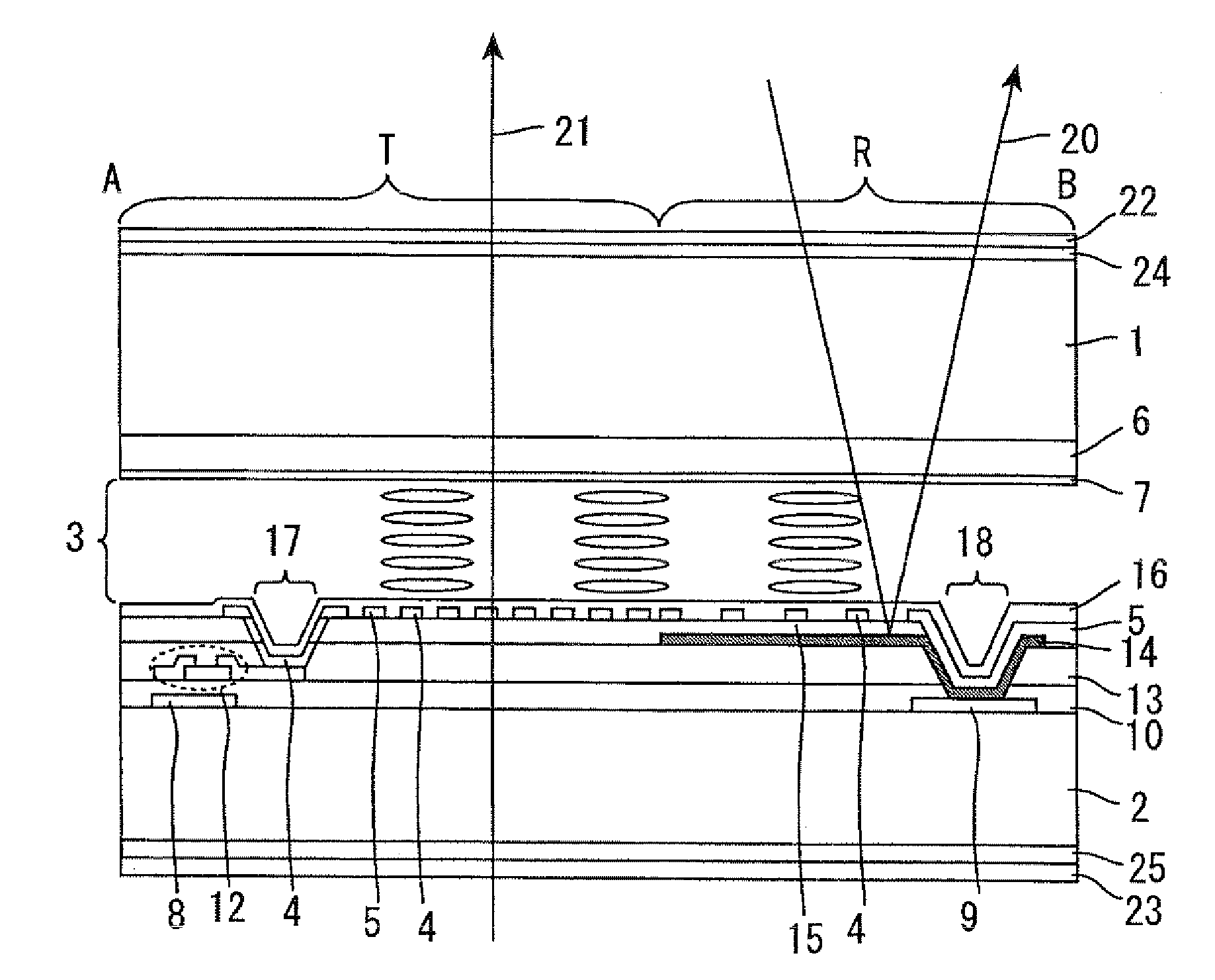
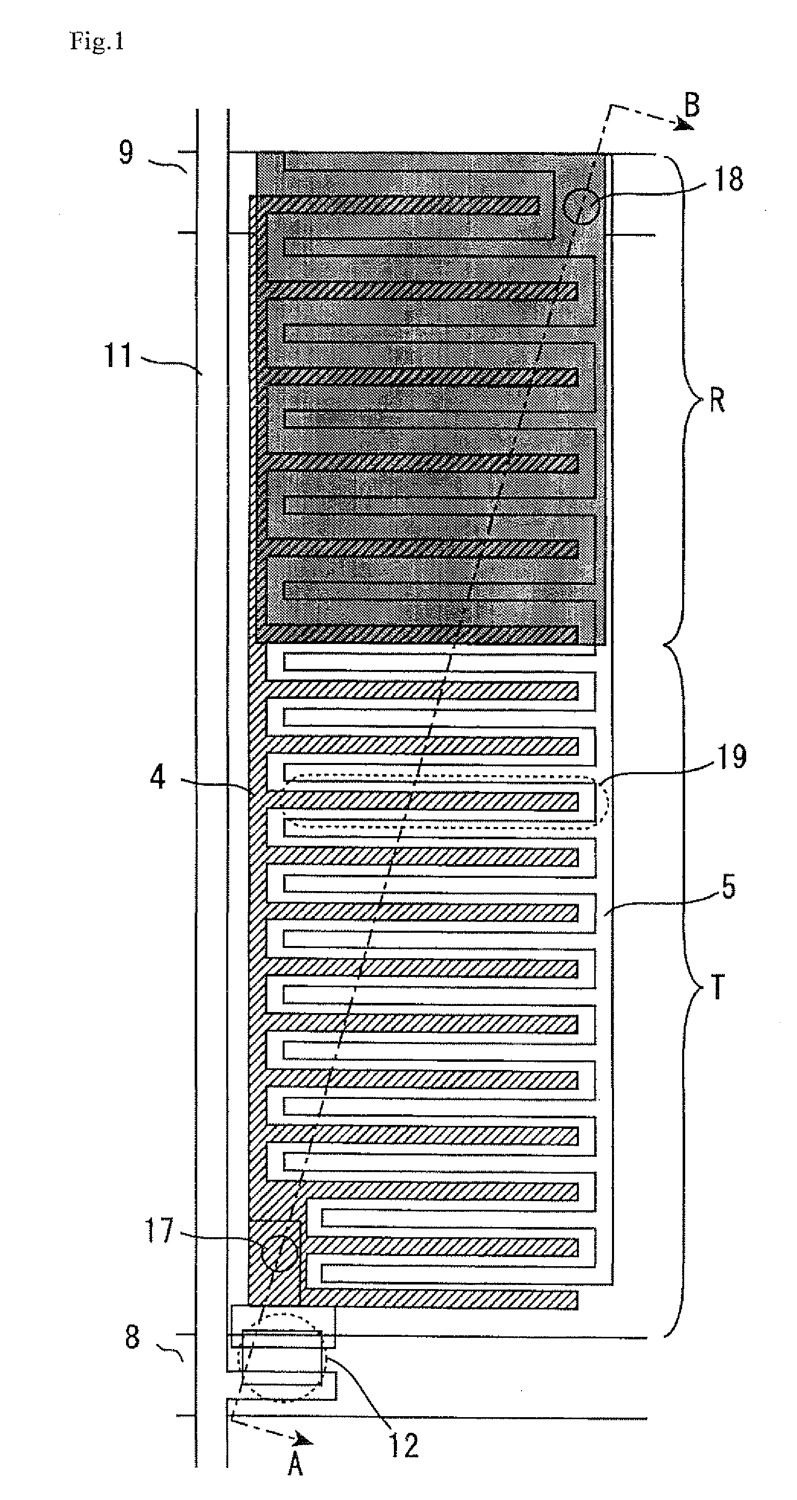
[0024]Embodiment 1 shows a liquid crystal display device in accordance with one embodiment of the display device of the present invention. FIG. 1 is a planar view schematically showing one pixel constituting the liquid crystal display device in Embodiment 1. FIG. 2 is a schematic view showing a cross section taken along dashed line A-B in FIG. 1. The liquid crystal display device in accordance with Embodiment 1 includes the first substrate 1, the second substrate 2, and a liquid crystal layer 3 interposed between these substrates, as shown in FIG. 2. The second substrate 2 includes a pixel electrode 4 and a common electrode 5, and a voltage is applied to the liquid crystal layer 3 through the pixel electrode 4 and the common electrode 5.
[0025]The first substrate 1 includes a color filter layer 6 and the first alignment film 7 on the liquid crystal layer 3 side in this order. A glass substrate can be used as the first substrate 1, for example. The color filter layer 6 includes red, g...
embodiment 2
[0040]Embodiment 2 shows a liquid crystal display device in accordance with one embodiment of the display device of the present invention. FIG. 12 is a planar view schematically showing one pixel constituting the liquid crystal display device in accordance with Embodiment 2. The liquid crystal display device in accordance with Embodiment 2 has the same configuration as in the liquid crystal display device in accordance with Embodiment 1, except for the arrangement relationship between the transmissive region T and the reflective region R (arrangement of the reflector) and the shape of the comb-tooth-shaped electrode (either or both of the pixel electrode 4 and the common electrode 5). As shown in FIG. 12, the transmissive region T and the reflective region R are arranged in such a way that the boundary between the two regions is parallel to the long-side of the pixel, in accordance with Embodiment 2. The region on the base side relative to the middle of the comb tooth of the pixel e...
embodiment 3
[0042]Embodiment 3 shows a liquid crystal display device in accordance with one embodiment of the display device of the present invention. FIG. 13 is a planar view schematically showing one pixel constituting a liquid crystal display device in accordance with Embodiment 3. FIG. 14 is a schematic view showing a cross section taken along dashed line A-B in FIG. 13. The liquid crystal display device in accordance with Embodiment 3 includes the first substrate 101, the second substrate 102, and a liquid crystal layer 103 interposed between these substrates, as shown in FIG. 14. The second substrate 102 includes a pixel electrode 104 and a common electrode 105. A voltage is applied to the liquid crystal layer 103 through the pixel electrode 104 and the common electrode 105.
[0043]The first substrate 101 includes a color filter layer 106 and the first alignment film 107 on the liquid crystal layer 103 side in this order. A glass substrate may be used as the first substrate 101, for example...
PUM
 Abstract
Description
Claims
Application Information