Liquid crystal display device

a liquid crystal display and vertical alignment technology, applied in static indicating devices, instruments, non-linear optics, etc., can solve the problems of significant decrease in aperture ratio, poor viewing angle characteristics, and large contrast and color changes, so as to suppress the decrease in transmittance in the intersection of the control electrode and the slit, suppress the decrease in transmittance in the intersection of the interconnection and the slit, and achieve no loss of aperture ratio

Active Publication Date: 2005-10-06
AU OPTRONICS CORP
View PDF6 Cites 33 Cited by
  • Summary
  • Abstract
  • Description
  • Claims
  • Application Information

AI Technical Summary

Benefits of technology

[0045] Moreover, if the control electrode is formed on an auxiliary capacitance bus line with an insulating film interposed therebetween, a display voltage supplied through the switching element can be more reliably maintained using the capacitance between the control electrode and the auxiliary capacitance bus line, and capacitances can be formed in the same region two-dimensionally. Accordingly, there is no loss of the aperture ratio. Furthermore, in the case where there are a plurality of sub picture element electrodes capacitively coupled to the control electrode, if a portion capacitively coupled to part of the sub picture element electrodes and a portion capacitively coupled to the rest of the

Problems solved by technology

However, TN liquid crystal display devices have the disadvantage that viewing angle characteristics are poor and that contrast and color greatly change when the screen is viewed from an oblique direction.
This causes a significant decrease in the aperture ratio.
This requires two steps for depositing transparent conductive material films and two steps for photolithography, and causes an increase in manufacturing cost.
However, dust occurring in rub

Method used


Image

  • Liquid crystal display device
  • Liquid crystal display device
  • Liquid crystal display device

Examples


first embodiment

[0083]FIG. 11 is a plan view showing a liquid crystal display device of a first embodiment of the present invention, and FIG. 12 is a cross-sectional schematic view thereof.

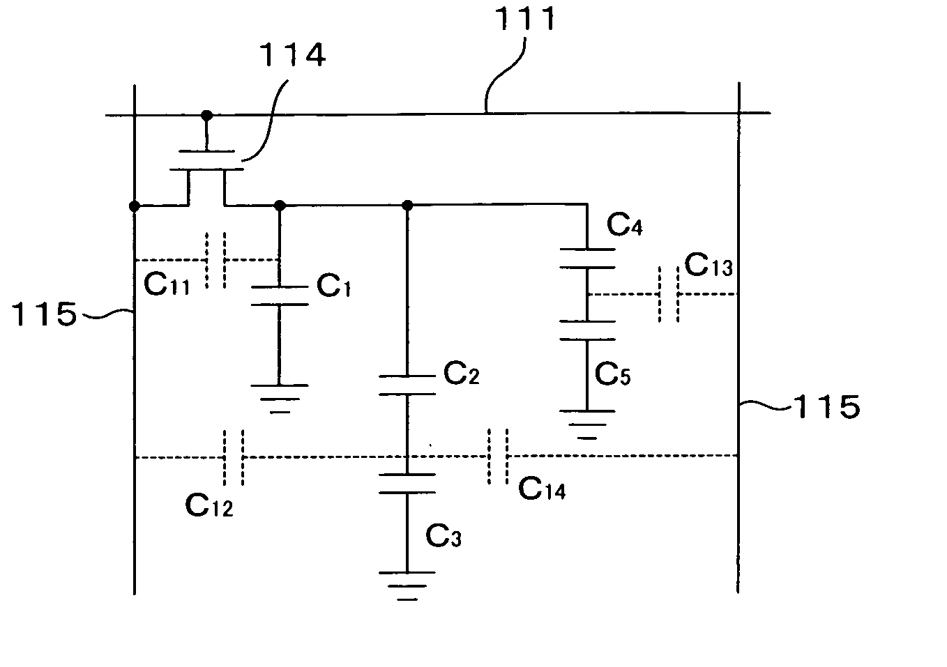
[0084] As shown in FIG. 12, the liquid crystal display device of the present embodiment includes two substrates 110 and 120 made of transparent thin plates, such as glass plates or the like, and vertical alignment-type liquid crystals (liquid crystals with negative dielectric anisotropy) contained between these substrates 110 and 120. As shown in FIG. 11, a plurality of gate bus lines 111 extending horizontally and a plurality of data bus lines 115 extending vertically are formed on the substrate 110. The pitch of the gate bus lines 111 is, for example, approximately 300 μm, and that of the data bus lines 115 is, for example, approximately 100 μm. Each of the rectangular regions defined by the gate bus lines 111 and the data bus lines 115 is a picture element region.

[0085] On the substrate 110, auxiliary capaci...

second embodiment

[0116]FIG. 14 is a plan view showing one picture element of a liquid crystal display device of a second embodiment of the present invention. In FIG. 14, the same components as those in FIG. 11 are denoted by the same reference numerals, and will not be further described in detail.

[0117] In the present embodiment, as shown in FIG. 14, the control electrode 113 and the sub picture element electrode 116c are electrically connected through a contact hole 132c formed in the second insulating film. Accordingly, if the voltage at the sub picture element electrode 116a is denoted by A, the voltage at the sub picture element electrode 116b is denoted by B, the voltage at the sub picture element electrode 116c is denoted by C, and the voltage at the sub picture element electrode 116d is denoted by D when a display voltage is supplied through the TFT 114, A=C=D>B is obtained.

[0118] In the first embodiment shown in FIG. 11, when a sufficiently high voltage is applied as a display voltage, the...

third embodiment

[0128]FIG. 17 is a plan view showing one picture element of a liquid crystal display device of a third embodiment of the present invention. The present embodiment differs from the first embodiment in that the shapes of sub picture element electrodes delimited by slits are different, but other components are basically the same as those of the first embodiment. Accordingly, in FIG. 17, the same components as those in FIG. 11 are denoted by the same reference numerals, and will not be further described in detail.

[0129] In the present embodiment, as shown in FIG. 17, a picture element electrode is divided into four sub picture element electrodes 151a, 151b, 151c, and 151d by slits 150a extending obliquely and slits 150b extending vertically. The sub picture element electrode 151a is horizontal-line symmetric. The shape of the sub picture element electrode 151a and the position thereof relative to the protrusion 124 are determined so that four regions (four domains) in which the orienta...


PUM


Abstract

A picture element electrode is divided into sub picture element electrodes by slits extending obliquely. Further, a control electrode is formed over an auxiliary capacitance bus line. Part of the sub picture element electrodes overlaps the control electrode and is capacitively coupled to the control electrode. The control electrode and the source electrode of a TFT are connected through an interconnection. Part of the sub picture element electrodes is electrically connected to the interconnection. Further, part of the sub picture element electrodes is electrically connected to an interconnection extending from the control electrode.

Description

CROSS-REFERENCE TO RELATED APPLICATIONS [0001] This application is based on and claims priority of Japanese Patent Application No.2004-106138 filed in Mar. 31, 2004, the entire contents of which are incorporated herein by reference. BACKGROUND OF THE INVENTION [0002] 1. Field of the Invention [0003] The present invention relates to a multi-domain vertical alignment (MVA) liquid crystal display device having a plurality of regions (domains) in which the orientations of liquid crystal molecules are different from each other. In particular, the present invention relates to a liquid crystal display device in which a picture element electrode is divided into a plurality of sub picture element electrodes. [0004] 2. Description of the Prior Art [0005] Liquid crystal display devices have the advantages that they are thin and light compared to cathode-ray tube (CRT) displays and that they can be operative at low voltages and have low power consumption. Accordingly, liquid crystal display dev...

Claims


Application Information

Patent Timeline
IPC IPC(8): G02F1/1337G02F1/133G02F1/1343G02F1/136G02F1/1368G09G3/36
CPCG02F1/134336G02F2001/134345G02F2001/134354G09G3/3607G09G2320/028G09G3/3648G09G2300/0443G09G2320/0209G09G2320/0242G09G3/3614G02F1/134345G02F1/134354G02F1/1343
Inventor KAMADA, TSUYOSHISASABAYASHI, TAKASHIUEDA, KAZUYAYOSHIDA, HIDEFUMI
Owner AU OPTRONICS CORP
Why Eureka
Try Eureka