Liquid crystal display device

Active Publication Date: 2009-05-21
PANASONIC LIQUID CRYSTAL DISPLAY CO LTD +1
View PDF5 Cites 38 Cited by
  • Summary
  • Abstract
  • Description
  • Claims
  • Application Information

AI Technical Summary

Benefits of technology

[0030]According to the present invention, in the IPS-method liquid crystal display device which includes the TFT substrate on which the pixel electrodes having the comb-teeth-shaped electrode and the slits and the planar common electrode are formed in an overlapping manner by way of the insulation film, an abnormal domain in the

Problems solved by technology

However, in the constitution disclosed in non-patent document 1, only the single electrode is used and hence, there is a large possibility of the disconnection of the pixel electrode.
Further, the formation of the pixel electrode int

Method used


Image

  • Liquid crystal display device
  • Liquid crystal display device
  • Liquid crystal display device

Examples


embodiment 1

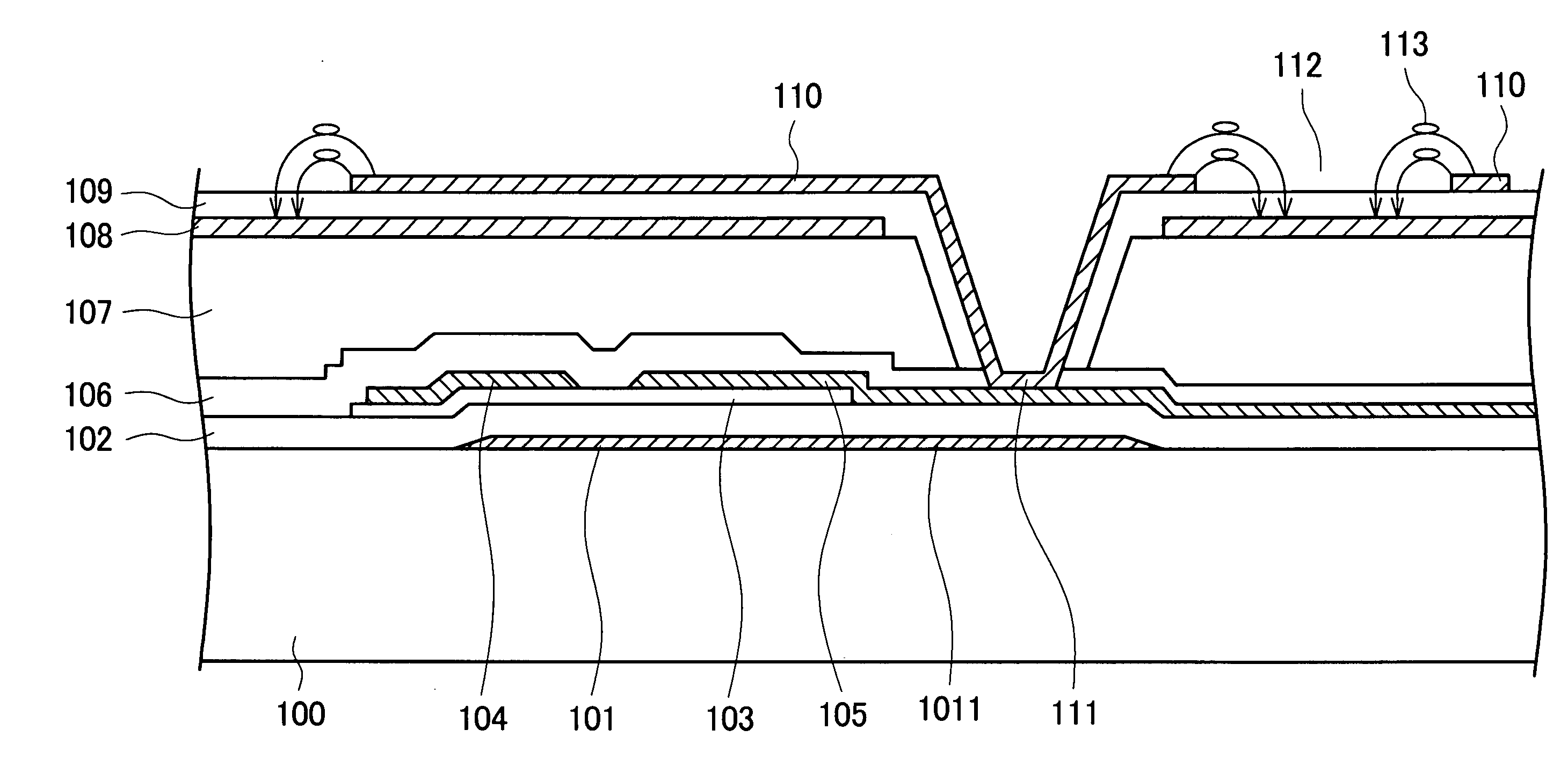
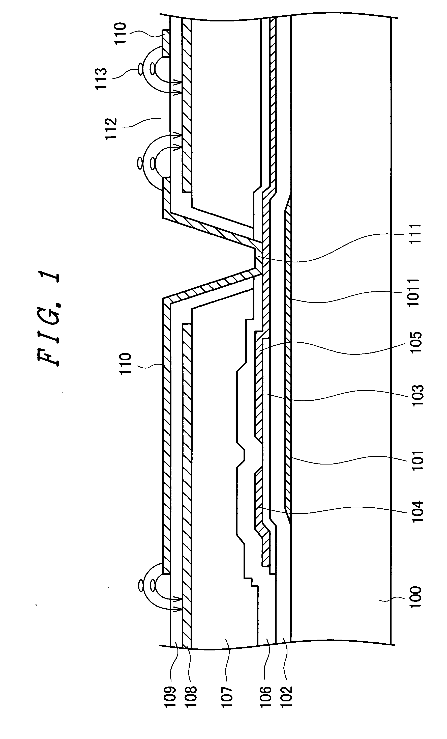
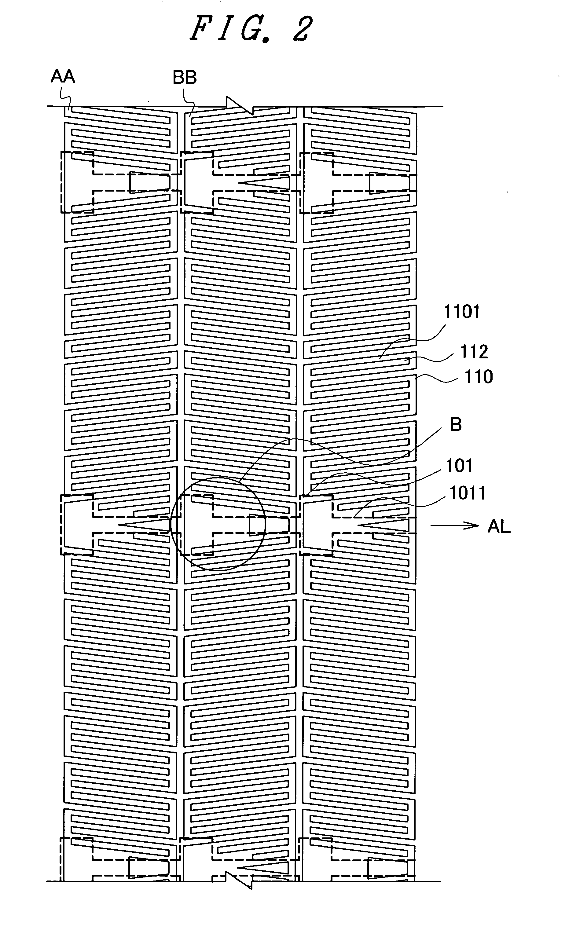
[0056]FIG. 2 is a plan view showing the arrangement of the pixels on the TFT substrate 100 of the embodiment 1. FIG. 3 is an enlarged view of a pixel AA shown in FIG. 2. FIG. 6 is an enlarged view of a pixel BB shown in FIG. 2. The pixel AA and the pixel BB are arranged in symmetry. FIG. 7 is an enlarged view showing a portion B shown in FIG. 2 in a see-through manner.

[0057]In FIG. 2, to prevent the drawing from becoming complicated, only the pixel electrodes 110 and the scanning line 1011 are shown. In FIG. 2, the pixel is formed in a laterally-extending trapezoidal shape. Conventionally, the pixel is defined by a region surrounded by video signal lines 1041 and scanning lines 1011. However, in this embodiment, the pixel is defined by the pixel electrode 110 per se. Further, the pixels are arranged in the longitudinal direction such that the pixel AA and the pixel BB are formed continuously thus providing the packed structure. Further, the pixels are also arranged in the lateral di...

embodiment 2

[0085]FIG. 10 is a plan view showing the arrangement of pixels of an embodiment 2 of the present invention. FIG. 10 shows the arrangement of the pixels, FIG. 11 is an enlarged view of a pixel electrode 110, and FIG. 12 is an enlarged view of an end portion of the pixel electrode 110. In FIG. 10, the pixels are defined or partitioned by scanning lines 1011 and video signal lines 1041. The pixel electrode 110 has a rectangular shape (however, being partially uneven around a through hole), wherein comb-teeth-shaped electrodes 1101 (slits 112) extend in a longitudinal direction and have distal ends thereof closed. Also in the arrangement of the pixels shown in FIG. 10, the cross-sectional constitution of the vicinity of the TFT is substantially equal to the cross-sectional constitution of the vicinity of the TFT in FIG. 1. In FIG. 10, the alignment direction of liquid crystal is a direction indicated by an arrow AL. Here, although the alignment direction of liquid crystal in the rectang...

embodiment 3

[0096]FIG. 16 is a plan view of the pixel electrode 110 showing a third embodiment of the present invention. The pixel electrode 110 shown in FIG. 16 has a laterally-extending trapezoidal shape, and a profile of the pixel electrode 110 is substantially equal to a profile of the corresponding pixel electrode 110 shown in FIG. 3. Further, the arrangement of the pixels is substantially equal to the corresponding arrangement of the pixels shown in FIG. 2 and hence, the arrangement of the pixels is omitted. That is, also in this embodiment, the pixels adopt the packed arrangement in the longitudinal direction as well as in the lateral direction. Although FIG. 16 shows only the pixel corresponding to the pixel of the first embodiment shown in FIG. 3, a pixel shape corresponding to the pixel shape shown in FIG. 6 appears in symmetry with the pixel shape shown in FIG. 16 and hence, the pixel shape corresponding to the pixel shape shown in FIG. 6 is omitted. The technical feature of the arra...


PUM


Abstract

An IPS-method liquid crystal display device which exhibits small directivity of a viewing angle and high brightness is realized. A planar common electrode is arranged below a pixel electrode which includes comb-teeth-shaped electrodes and slits. When a video signal is applied to the pixel electrode, an electric field is generated between the pixel electrode and the common electrode by way of slit portions formed in the pixel electrode thus controlling liquid crystal molecules. To reduce the occurrence of a phenomenon that an abnormal domain is generated in an end portion of the slit and the abnormal domain lowers transmissivity of liquid crystal, the structure in which the slits having both ends thereof closed and the slits having one-side end portion thereof opened are alternately arranged next to each other in parallel is adopted.

Description

[0001]The present application claims priority from Japanese application JP2007-299271 filed on Nov. 19, 2007, the content of which is hereby incorporated by reference into this application.BACKGROUND OF THE INVENTION[0002]1. Field of the Invention[0003]The present invention relates to a liquid crystal display device, and more particularly to a lateral-electric-field liquid crystal display device which exhibits excellent viewing angle characteristic and brightness characteristic.[0004]2. Background Art[0005]A liquid crystal display device includes a TFT substrate on which pixel electrodes, thin film transistors (TFT) and the like are formed in a matrix array and a counter substrate which forms color filters or the like thereon at places where the color filters faces the pixel electrodes in an opposed manner, and liquid crystal is sandwiched between the TFT substrate and the counter substrate. Further, an image is formed by controlling transmissivity of light for every pixel by drivin...

Claims


Application Information

Patent Timeline
IPC IPC(8): G02F1/136
CPCG02F1/133707G02F2001/134381G02F2001/134372G02F1/134363G02F1/134381G02F1/134372
Inventor TANNO, JUNJI
Owner PANASONIC LIQUID CRYSTAL DISPLAY CO LTD
Why Eureka
Try Eureka