Manufacturing method of tft array substrate

A manufacturing method and array substrate technology, applied in semiconductor/solid-state device manufacturing, semiconductor devices, electrical components, etc., can solve the problems of conductive film 9' rupture, affect panel display effect, and unreliable resistance bridging, etc., to improve product quality. Yield rate, improved display effect, bridging reliable effect

Active Publication Date: 2019-04-02
SHENZHEN CHINA STAR OPTOELECTRONICS SEMICON DISPLAY TECH CO LTD
View PDF5 Cites 0 Cited by
  • Summary
  • Abstract
  • Description
  • Claims
  • Application Information

AI Technical Summary

Problems solved by technology

[0007] like Figure 4 , Figure 5 As shown, the process of making the via hole V' in the prior art is as follows: first, use a traditional full tone mask (Full Tone Mask) FTM to expose, and remove all the photoresist PR on the area where the via hole V' is to be formed; then Use the remaining photoresist PR as a shielding layer to perform dry etching on the protective layer PV and the gate insulating layer GI. Due to the blocking of the second metal layer M2 to dry etching and the chemical etching characteristics of dry etching, the TFT T3 The gate insulating layer GI at the tapper of the drain D3 is prone to undercut (Under-cut) ( Figure 5 The area shown by the dashed circle), forming a sharp corner
In the subsequent deposition process of conductive thin film 9', such as image 3 As shown, the undercut of the gate insulating layer GI is likely to cause the conductive film 9' to break, resulting in high resistance and unreliable bridging between the drain D3 of the discharge TFT T3 and the common voltage line Com, thereby affecting the display of the panel effect, resulting in a decrease in product yield

Method used


Image

  • Manufacturing method of tft array substrate
  • Manufacturing method of tft array substrate
  • Manufacturing method of tft array substrate

Examples


Embodiment Construction

[0040] In order to further illustrate the technical means adopted by the present invention and its effects, the following describes in detail in conjunction with preferred embodiments of the present invention and accompanying drawings.

[0041] The invention provides a method for manufacturing a TFT array substrate, comprising the following steps:

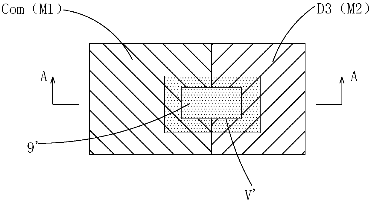
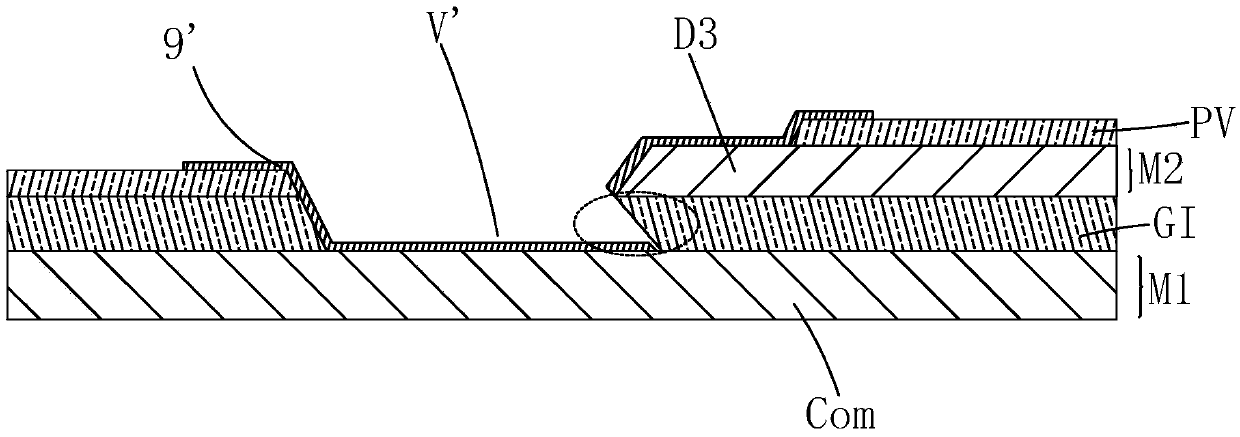
[0042] Step S1, please refer to Image 6 , combined with Figure 12 On the substrate 1, a first metal layer M1, a gate insulating layer GI, a semiconductor active layer 2, a second metal layer M2, and a protection layer PV are sequentially formed from bottom to top, and a photoresist is coated on the protection layer PV. PR.

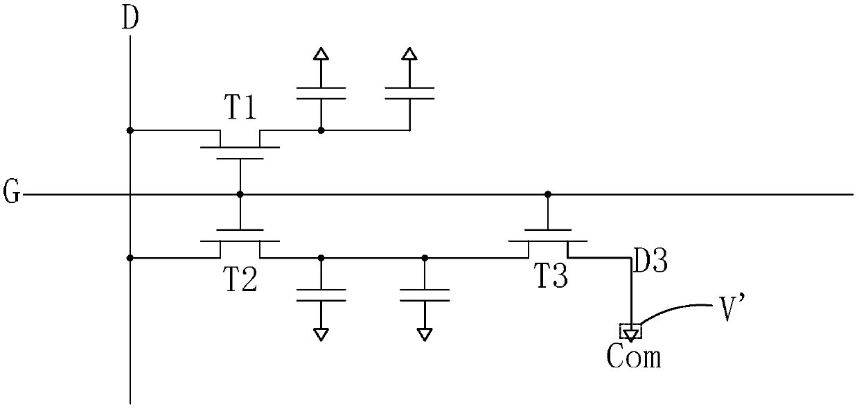
[0043] The gate insulating layer GI covers the first metal layer M1, and the first metal layer M1 includes a gate line G and a common voltage line Com;

[0044] The protection layer PV covers the second metal layer M2, and the second metal layer M2 includes a data line D, a first source S1, a first drain D1,...


PUM


Abstract

Provided is a method for manufacturing a TFT array substrate. The method comprises: taking a half-tone mask plate (3) as a tool for exposure, so that a drain electrode (D3) of a discharging TFT (T3) in a second metal layer (M2) and an upper part of a climbing position thereof reserve a thin layer of a photoresistor (PR); and the reserved thin layer of the photoresistor (PR) protecting a gate insulation layer (GI) under the climbing position of the drain electrode (D3) of the discharging TFT (T3) in a subsequent dry-etching process, preventing the gate insulation layer (GI) from having the problems of over-etching and undercutting at the climbing position of the drain electrode (D3) of the discharging TFT (T3) because of material differences, reducing the risk of a conductive thin film (9) fracturing, enabling the bridging between the drain electrode (D3) of the discharging TFT (T3) and a common voltage line (Com) to be reliable, and not reducing the aperture ratio, and thereby improving the display effect of a panel and enhancing the product yield.

Description

technical field [0001] The invention relates to the field of display technology, in particular to a method for manufacturing a TFT array substrate. Background technique [0002] Thin Film Transistor Liquid Crystal Display (TFT-LCD) can display high-definition, continuous, and delicate images, and is more and more popular among consumers. [0003] The existing TFT-LCDs on the market generally include a housing, a liquid crystal panel disposed in the housing, and a backlight module disposed in the housing. The liquid crystal panel is composed of a color filter (Color Filter, CF) substrate, a thin film transistor array substrate (ThinFilm Transistor Array Substrate, TFT Array Substrate), and a liquid crystal layer (Liquid Crystal Layer) arranged between the two substrates. The working principle is to control the rotation of the liquid crystal molecules in the liquid crystal layer by applying a driving voltage on the two glass substrates, and refract the light from the backligh...

Claims


Application Information

Patent Timeline
Patent Type & Authority Patents(China)
IPC IPC(8): H01L21/77H01L27/12
CPCH01L27/1288
Inventor 王勐
Owner SHENZHEN CHINA STAR OPTOELECTRONICS SEMICON DISPLAY TECH CO LTD
Why Eureka
Try Eureka