Reticle fabrication using a removable hard mask

a technology of hard mask and reticle, which is applied in the direction of semiconductor/solid-state device testing/measurement, instruments, photomechanical equipment, etc., can solve the problems of reducing the critical dimension size of the tool used for reticle fabrication, reducing the critical dimension size, and reducing the critical dimension bias

Inactive Publication Date: 2005-08-04
APPLIED MATERIALS INC
View PDF8 Cites 24 Cited by
  • Summary
  • Abstract
  • Description
  • Claims
  • Application Information

AI Technical Summary

Benefits of technology

[0015] We have reduced the critical dimension bias for reticle fabrication. Pattern transfer to the radiation-blocking layer of the reticle substrate essentially depends upon transfer from a hard mask rather than from a photoresist. The photoresist pull back which occurs during pattern transfer to the hard mask is minimal and the change in the critical dimension between the photoresist pattern and the hard mask pattern is typically less than about 10-12 nm. In addition, when the hard mask material has anti-reflective properties which are tailored to the imaging radiation wavelength, the reflectivity from the chrome surface is substantially reduced during imaging of the photoresist, which further reduces the change in critical dimension between the direct write pattern and the pattern transferred to the hard mask. When the selectivity during transfer of the pattern from the hard mask to the radiation-blocking layer is high, typically at least about 5:1 (where the radiation-blocking layer etches 5 times faster than the hard mask), this further reduces the critical dimension bias (typically referred to as etch bias) in the pattern transferred to the chrome (or other radiation-blocking layer). The highest selectivity for the radiation-blocking layer relative to the hard mask, which can be obtained while meeting other requirements for the hard mask, is advantageous. A combination of the above-described process considerations enables a reduction in critical dimension size of the patterned radiation-blocking layer and provides an improvement in the pattern feature integrity of the patterned radiation-blocking layer. A typical increase in critical dimension from the size of the direct write pattern radiation to the patterned radiation-blocking layer may be in the range of about 5% to 7% or less.
[0016] In one embodiment of the invention, a hard mask material having anti-reflective properties may be left on the surface of the chrome after etching of the chrome. Since the hard mask surface faces the surface of a photoresist on the semiconductor substrate which is patterned using the reticle, the presence of the proper anti-reflective properties in the hard mask can be used to reduce the amount of bounce-back of reflected radiation which occurs during blanket radiation imaging of the semiconductor photoresist through the reticle. By bounce back reflected radiation, it is meant the radiation which reflects off the semiconductor substrate to the reticle or to other surfaces (between the reticle and the semiconductor substrate) and then back to the semiconductor substrate photoresist.
[0017] In another embodiment of the invention, where a wet etch is used during fabrication of the reticle, the hard mask material (whether having anti-reflective properties or not) is removed to prevent contamination during the wet etch process. In this embodiment, when a plasma etchant used to remove the hard mask would also etch the reticle base substrate (which is typically quartz), a protective layer is applied to fill at least a portion of patterned openings through the chrome during removal of the hard mask. This prevents etching of the quartz at the bottom of the pattern openings during removal of the hard mask.

Problems solved by technology

However, the anti-reflective properties of this layer are not as effective for present day photoresist imaging radiation as they were for imaging radiation which was used with earlier photoresists used in the art of reticle fabrication.
However, since the reticle is subsequently used in a manner where imaging radiation will come down through the top and out the bottom, there cannot be any significant scratches on either surface of the reticle through which the radiation will pass.
As a result, the tool used for reticle fabrication requires specialized reticle substrate handling devices and contact surfaces.
However, since 30 nm cannot be written, the phase shift is limited to the threshold of what can be written.

Method used


Image

  • Reticle fabrication using a removable hard mask
  • Reticle fabrication using a removable hard mask
  • Reticle fabrication using a removable hard mask

Examples


example embodiments

Example One

example two

Avoiding the Photoresist Pull Back Problem

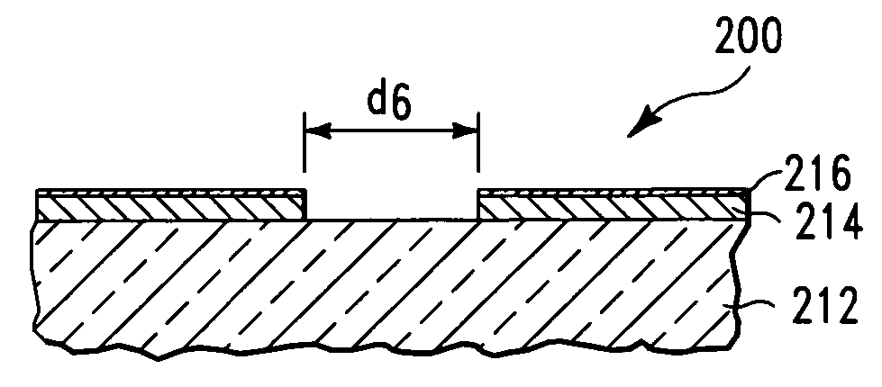
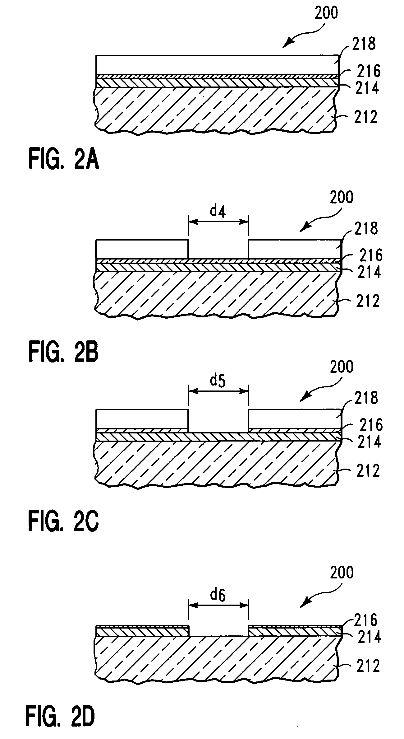
[0045]FIGS. 2A through 2D illustrate the general concept which permits pattern etching of the radiation-blocking layer of a reticle without photoresist pull back, and thus without the resulting CD bias problems. FIGS. 2A through 2D show schematic cross-sectional views of a reticle fabrication process beginning with a starting structure and ending with the patterned reticle.

[0046]FIG. 2A shows the reticle starting structure 200 which consists of, from top to bottom, a chemically amplified photoresist layer 218 of the kind described with reference to FIGS. 1A through 1C; the thickness of the photoresist layer 218 was about 3,000 Å to about 4,000 Å. Underlying photoresist layer 218 was a layer of inorganic ARC, SixOyNz 216 which was selected to function as a plasma etching hard mask having anti-reflective properties. The thickness of the SixOyNz, hard mask layer 216 ranged from about 200 Å to about 500 Å, and was typically about 300 Å. Underl...

example three

Advantage of a Reticle Having an ARC over the Patterned Radiation-Blocking Layer

[0061]FIGS. 3A through 3D illustrate schematic cross-sectional views which show the advantages of a reticle structure where a hard mask having antireflective properties is present over the surface of a patterned chrome-containing layer (or other radiation-blocking layer) during imaging of a photoresist on a semiconductor wafer using the reticle. This feature is helpful when imaging of the photoresist is with optical radiation.

[0062]FIG. 3A shows a schematic cross-sectional view of a reticle structure 305 including, from bottom to top, a quartz substrate 312, underlying a patterned chrome-containing radiation-blocking layer 314, with an inorganic layer having anti-reflective properties 316 present on the upper surface of the patterned radiation-blocking layer 314. This structure is of the kind shown in FIG. 3D above, the fabrication of which is described in detail with reference to FIG. 3D.

[0063]FIG. 3...


PUM

PropertyMeasurementUnit
wavelengthaaaaaaaaaa
wavelength rangingaaaaaaaaaa
thickaaaaaaaaaa

Abstract

We have reduced the critical dimension bias for reticle fabrication. Pattern transfer to the radiation-blocking layer of the reticle substrate essentially depends upon use of a hard mask to which the pattern is transferred from a photoresist. The photoresist pull back which occurs during pattern transfer to the hard mask is minimalized. In addition, a hard mask material having anti-reflective properties which are matched to the reflective characteristics of the radiation-blocking layer enables a reduction in critical dimension size and an improvement in the pattern feature integrity in the hard mask itself. An anti-reflective hard mask layer left on the radiation-blocking layer provides functionality when the reticle is used in a semiconductor device manufacturing process.

Description

BACKGROUND OF THE INVENTION [0001] 1. Field of the Invention [0002] The present invention relates to a method used to fabricate a reticle, which is also commonly referred to as a photomask. The reticle includes a patterned layer through which radiation passes during the transfer of the pattern from the reticle to a substrate via photolithographic techniques. [0003] 2. Description of the Background Art [0004] A typical reticle fabrication process begins with the formation of a substrate which typically includes a silicon-containing base layer such as a quartz layer, with a layer of chrome applied over the quartz, and a layer of chrome oxide transitioning to chrome oxynitride which is formed over the chrome layer. A photoresist material is commonly applied over the chrome oxide / chrome oxynitride layer. The photoresist material is pattern imaged by irradiation, and the image in the photoresist is developed into a pattern. Then the patterned photoresist is used as a mask for transferrin...

Claims


Application Information

Patent Timeline
Patent Type & Authority Applications(United States)
IPC IPC(8): G03F1/08G03F7/09
CPCG03F1/80G03F1/68G03F1/46G03F1/72G03F7/09
Inventor BENCHER, CHRISTOPHER DENNISMONTGOMERY, MELVIN WARRENBUXBAUM, ALEXANDERLEE, YUNG-HEE YVETTEDING, JIANALMOGY, GILADYEH, WENDY H.
Owner APPLIED MATERIALS INC
Why Eureka
Try Eureka