Method of reducing critical dimension bias during fabrication of a semiconductor device
a semiconductor device and critical dimension technology, applied in the field of critical dimension bias reduction during reticle fabrication, can solve the problems of not being able to pass light through the reticle through any significant scratches on either surface of the reticle, and the critical dimension size is reduced. , the effect of reducing the critical dimension siz
- Summary
- Abstract
- Description
- Claims
- Application Information
AI Technical Summary
Benefits of technology
Problems solved by technology
Method used
Image
Examples
example embodiments
Example One
example two
Avoiding the Photoresist Pull Back Problem
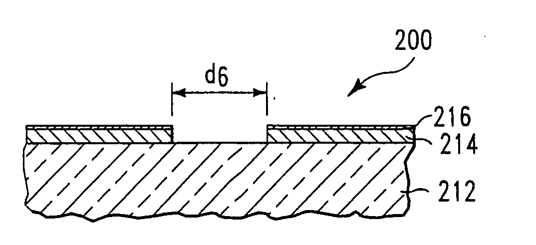
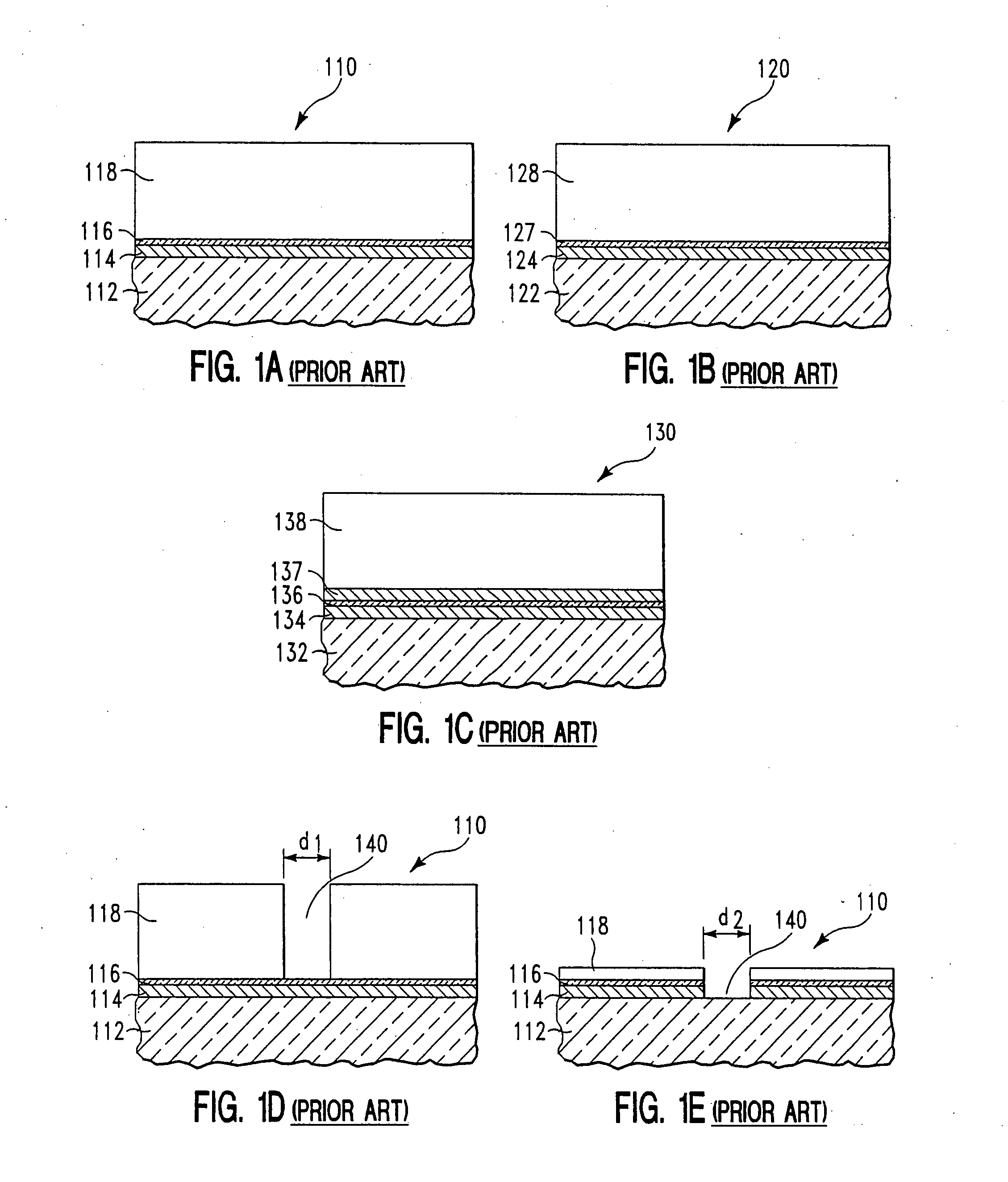
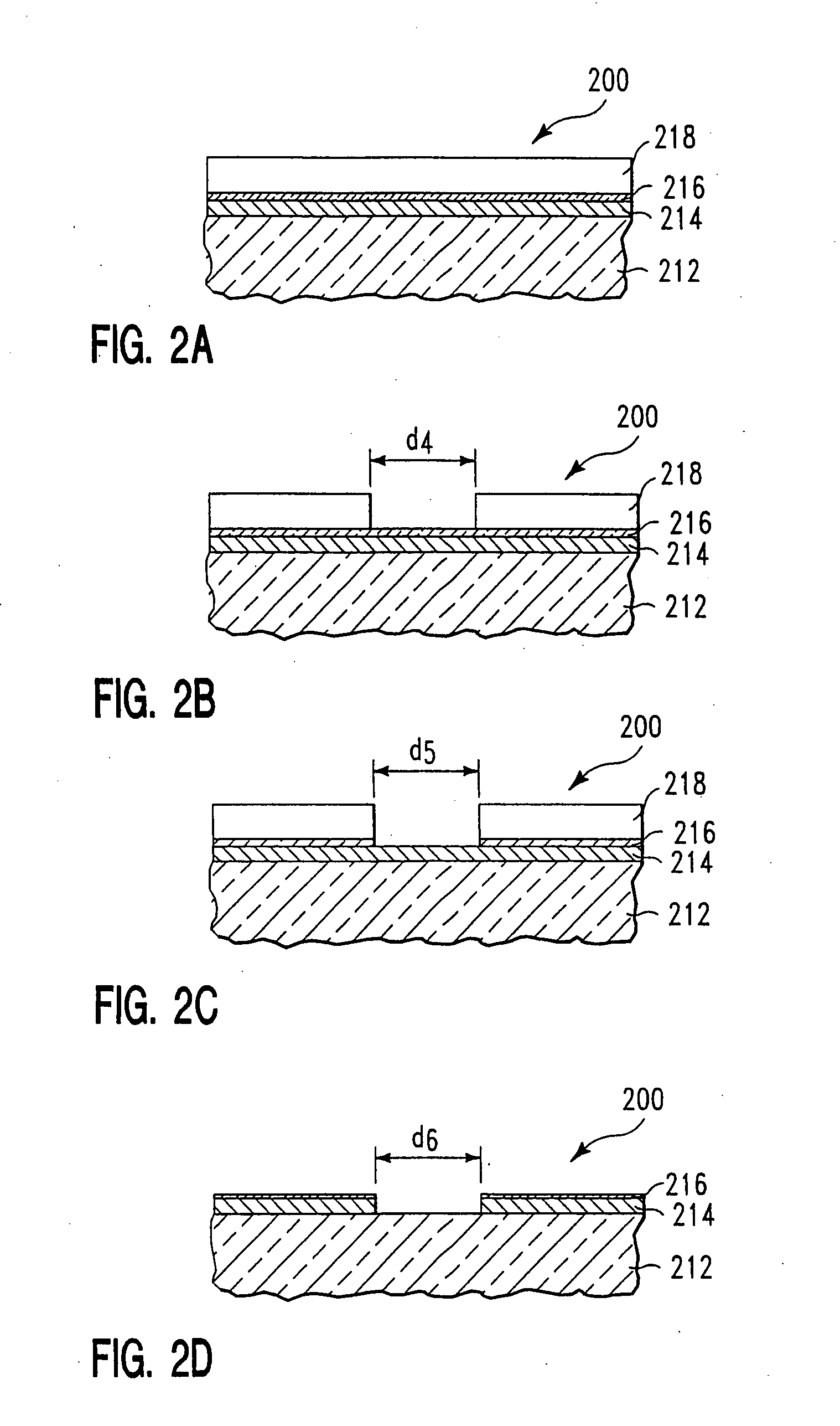
[0047]FIGS. 2A through 2D illustrate the general concept which permits pattern etching of the radiation-blocking layer of a reticle without photoresist pull back, and thus without the resulting CD bias problems. FIGS. 2A through 2D show schematic cross-sectional views of a reticle fabrication process beginning with a starting structure and ending with the patterned reticle.
[0048]FIG. 2A shows the reticle starting structure 200 which consists of, from top to bottom, a chemically amplified photoresist layer 218 of the kind described with reference to FIGS. 1A through 1C; the thickness of the photoresist layer 218 was about 3,000 Å to about 4,000 Å. Underlying photoresist layer 218 was a layer of inorganic ARC, SixOyNz 216 which was selected to function as a plasma etching hard mask having anti-reflective properties. The thickness of the SixOyNz, hard mask layer 216 ranged from about 200 Å to about 500 Å, and was typically about 300 Å. Underl...
example three
Advantage of a Reticle Having an ARC Over the Patterned Radiation-Blocking Layer
[0066]FIGS. 3A through 3D illustrate schematic cross-sectional views which show the advantages of a reticle structure where a hard mask having antireflective properties is present over the surface of a patterned chrome-containing layer (or other radiation-blocking layer) during imaging of a photoresist on a semiconductor wafer using the reticle. This feature is helpful when imaging of the photoresist is with optical radiation.
[0067]FIG. 3A shows a schematic cross-sectional view of a reticle structure 305 including, from bottom to top, a quartz substrate 312, underlying a patterned chrome-containing radiation-blocking layer 314, with an inorganic layer having anti-reflective properties 316 present on the upper surface of the patterned radiation-blocking layer 314. This structure is of the kind shown in FIG. 3D above, the fabrication of which is described in detail with reference to FIG. 3D.
[0068]FIG. 3...
PUM
| Property | Measurement | Unit |
|---|---|---|
| thick | aaaaa | aaaaa |
| wavelength | aaaaa | aaaaa |
| wavelength | aaaaa | aaaaa |
Abstract
Description
Claims
Application Information


