Separated gate type memory embedded into logic circuit and manufacturing method of memory group

A technology of separating gates and manufacturing methods, which is applied in the manufacture of circuits, electrical solid-state devices, semiconductor/solid-state devices, etc., can solve problems such as memory operating speed signal transmission bandwidth limitations, and achieve increased density, small integrated chips, and high operating speed fast effect

Active Publication Date: 2013-03-06
SEMICON MFG INT (SHANGHAI) CORP
View PDF3 Cites 24 Cited by
  • Summary
  • Abstract
  • Description
  • Claims
  • Application Information

AI Technical Summary

Problems solved by technology

[0005] If split-gate flash memory, high-voltage transistors, and logic transistors are all built on discrete integrated chips, the operating speed of the entire memory will be limited by the signal transmission bandwidth between the flash memory and peripheral circuits

Method used


Image

  • Separated gate type memory embedded into logic circuit and manufacturing method of memory group
  • Separated gate type memory embedded into logic circuit and manufacturing method of memory group
  • Separated gate type memory embedded into logic circuit and manufacturing method of memory group

Examples


no. 2 example

[0082] Figure 15 Shown is a flow chart of a manufacturing method of a split-gate flash memory group embedded with logic circuits according to the second embodiment of the present invention. The group of split-gate flash memories with embedded logic circuits includes a pair of split-gate flash memories with embedded logic circuits of the same size, and each pair of split-gate flash memories with embedded logic circuits includes: Split gate flash memory, high voltage transistors, logic transistors. The fabrication method below takes a pair of split-gate flash memories embedded with logic circuits as an example. Same as the first embodiment, the split-gate flash memory with erase gate and word line gate is still taken as an example.

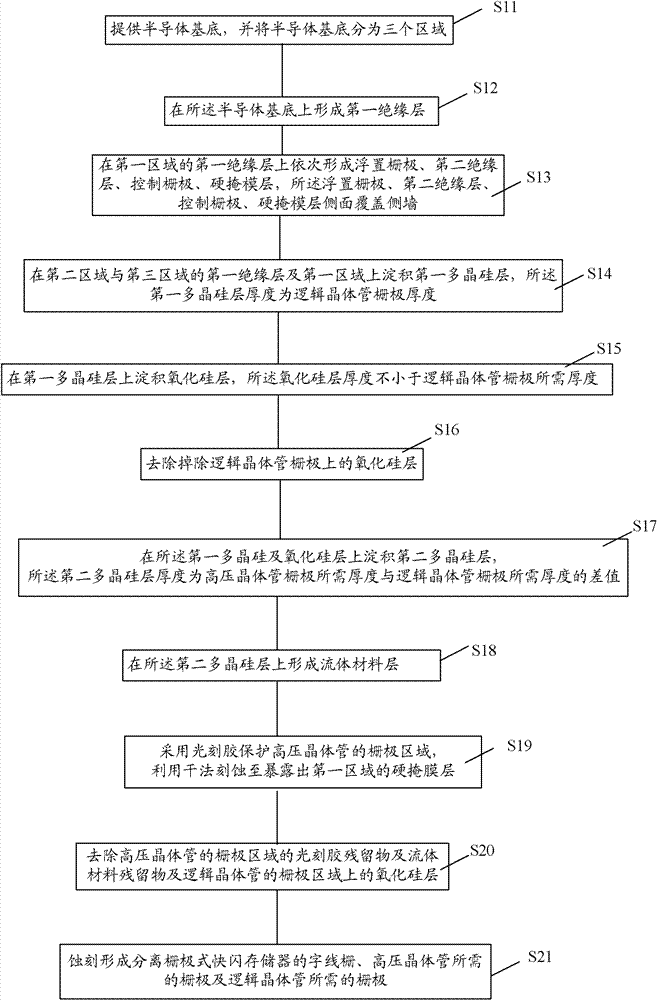
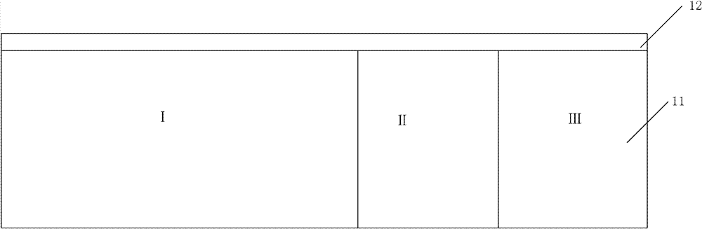
[0083] Step S11' is executed to provide a semiconductor substrate 11', which includes six regions for forming a pair of identical split-gate flash memories embedded with logic circuits, such as Figure 16 As shown, the six regions are specifical...


PUM


Abstract

The invention provides a manufacturing method of separated gate type flash memories embedded into logic circuits. Compared with a method of separately manufacturing the separated gate type flash memories, the manufacturing method includes four additional steps of once more polycrystalline deposition, once more silicon oxide deposition, once more etching and once more fluid coverage. The characteristic of good fluidity of fluid materials is utilized, grooves, especially deep grooves can be filled, and areas required to be protected can be prevented from being etched in the etching step. The separated gate type flash memories manufactured by the method are embedded into peripheral circuits of high-voltage transistors and logic transistors so that the separated gate type flash memories, the high-voltage transistors and the logic transistors can be manufactured on one integrated circuit, and the integration of the separated gate type flash memories, the high-voltage transistors and the logic transistors is high in density and quick in running. Further, integrated chips are smaller so that cost of each integrated chip is lowered.

Description

technical field [0001] The invention relates to the technical field of semiconductors, in particular to a separate gate type flash memory embedded in a logic circuit and a manufacturing method of the memory group. Background technique [0002] Random access memory, such as DRAM and SRAM, has the problem of data loss after power failure during use. To overcome this problem, various nonvolatile memories have been designed and developed. Recently, flash memory based on the floating gate concept has become the most versatile non-volatile memory due to its small cell size and good performance. The non-volatile memory mainly includes two basic structures: a stack gate structure and a split gate structure. The stacked gate structure memory includes a tunnel oxide layer formed on the substrate, a floating gate polysilicon layer (ploy 1) for storing electrons, an oxide / nitride / oxide (oxide-nitride-oxide, ONO ) stack and control gate polysilicon layer (ploy 2) that controls electro...

Claims


Application Information

Patent Timeline
Patent Type & Authority Applications(China)
IPC IPC(8): H01L21/8247H01L27/115
Inventor 王友臻洪中山周儒领
Owner SEMICON MFG INT (SHANGHAI) CORP
Why Eureka
Try Eureka