Self-alignment of metal and via using selective deposition

a technology of selective deposition and self-alignment, which is applied in the direction of basic electric elements, semiconductor/solid-state device manufacturing, electric apparatus, etc., can solve the problems of limiting the pitch or spacing between exposed features, the critical dimension (cd) or resolution of patterned features is becoming more difficult to produce, and the challenge of photolithographic misalignment,

Active Publication Date: 2017-12-05
TOKYO ELECTRON LTD
View PDF5 Cites 23 Cited by
  • Summary
  • Abstract
  • Description
  • Claims
  • Application Information

AI Technical Summary

Benefits of technology

[0007]Techniques herein include methods of patterning substrates such as for back end of line (BEOL) metallization processes. Techniques herein enable fully self-aligned vias and lines. Processes herein include using selective deposition, protective films and combination etch masks for accurately patterning a substrate.
[0010]The second relief pattern is transferred into the dielectric layer by using the second relief pattern as a first etch mask and etching through the dielectric layer stopping on the conformal film above the first metal lines. The conformal film preventing etching of the second dielectric lines and the first metal lines uncovered by the second relief pattern. The first relief pattern is transferred into the dielectric layer by using the first relief pattern as a second etch mask and etching into the dielectric layer stopping on top surfaces of the second dielectric lines using the conformal film as an etch stop layer. Subsequently, the relief patterns can be removed, and the substrate metallized having fully self-aligned vias.

Problems solved by technology

Conventional lithographic techniques for exposing a pattern of radiation or light onto a substrate have various challenges that limit a size of features exposed, and limit pitch or spacing between exposed features.
As smaller devices are fabricated, the critical dimension (CD) or resolution of patterned features is becoming more challenging to produce.
On top of that concern, an additional challenge is that of overlay such as photolithographic misalignment.
If masks and patterns are not properly aligned, then device defects and failures can occur as lines are either partially cut or not cut at desired locations, or as openings are misplaced or shorts are otherwise created.
Such misalignment is a challenge with metallization of substrates as multiple layers of metal lines and vias interconnect transistors.
Not only is overlay a challenge, but another challenge with metallization is creating trenches and vias without damaging surrounding dielectric material.

Method used


Image

  • Self-alignment of metal and via using selective deposition
  • Self-alignment of metal and via using selective deposition
  • Self-alignment of metal and via using selective deposition

Examples


Embodiment Construction

[0026]Techniques herein include methods of patterning substrates such as for back end of line (BEOL) metallization processes. Techniques herein enable fully self-aligned vias and lines. Processes herein include using selective deposition, protective films and combination etch masks for accurately patterning a substrate. Such combinations mitigate overlay errors by using underlying structures to self-align patterns, and protect sensitive dielectric materials from being degraded.

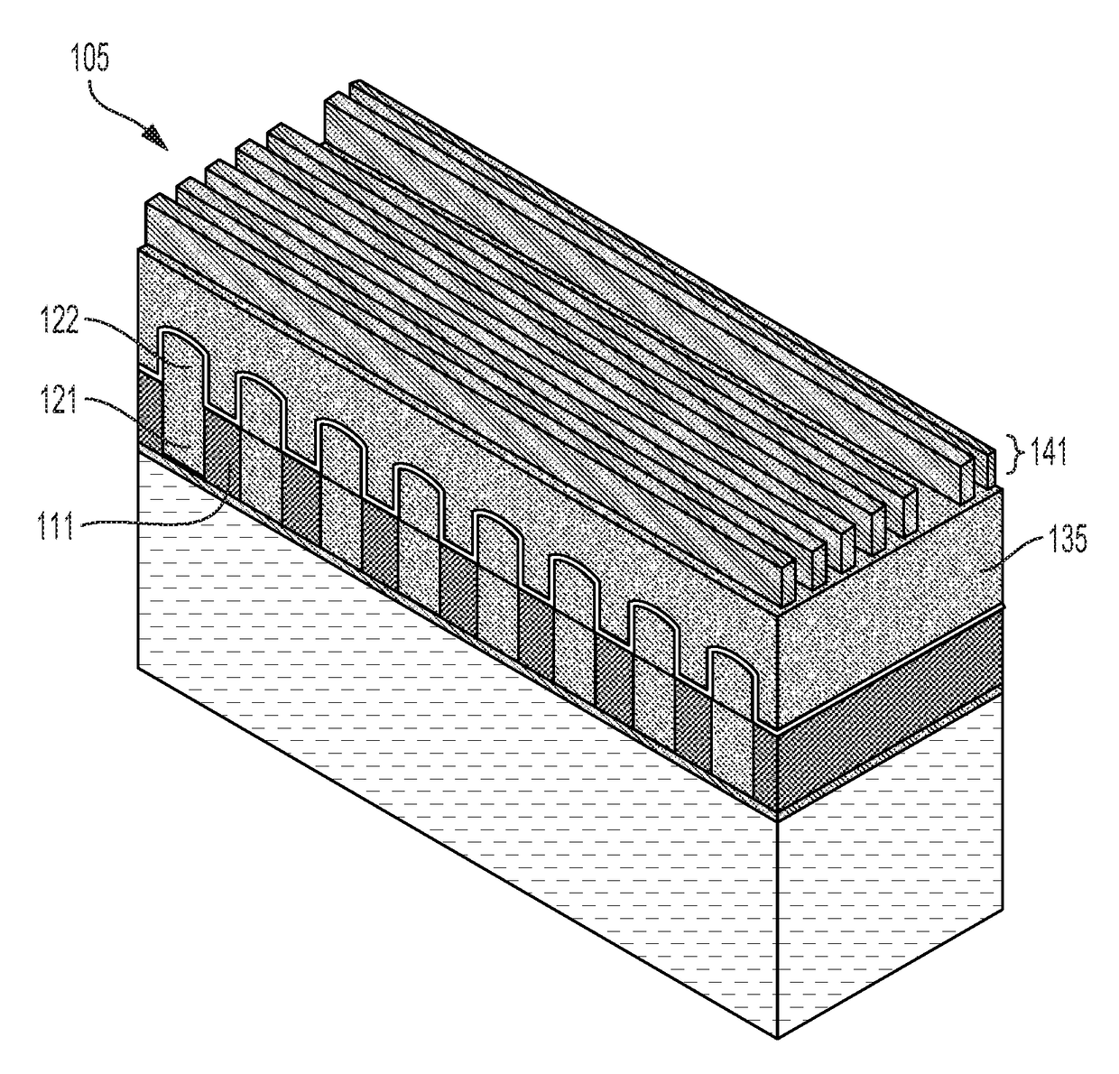
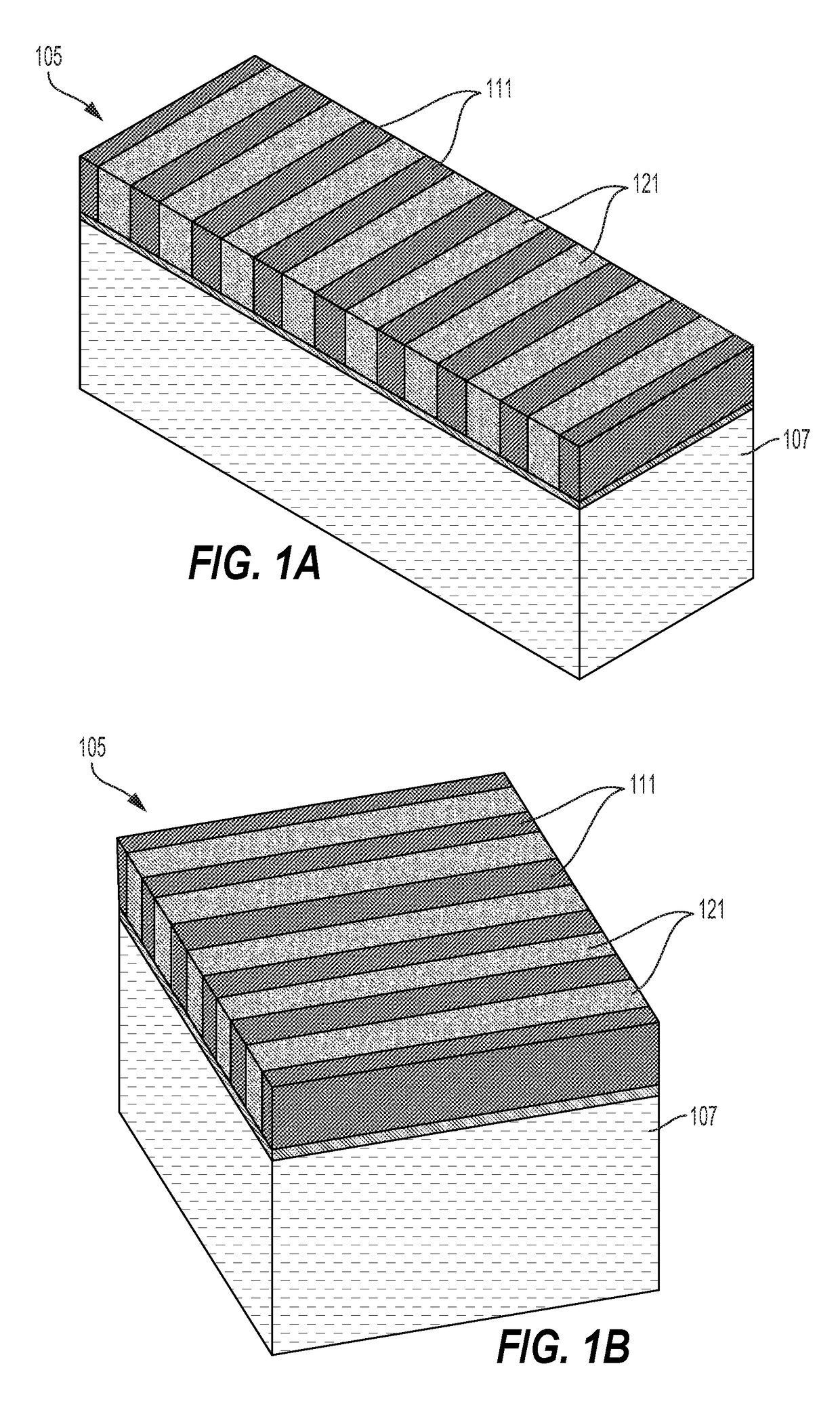
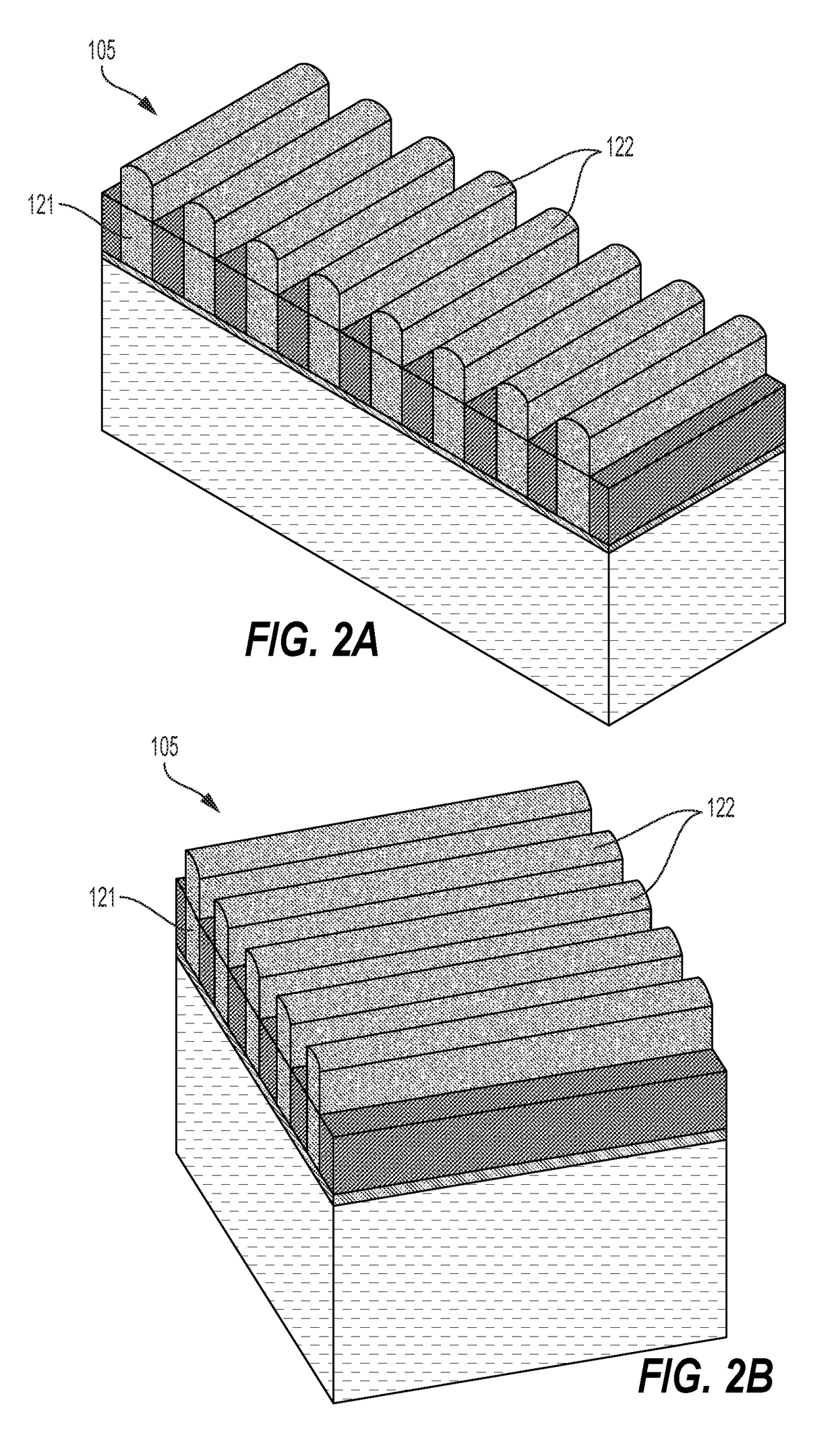
[0027]One embodiment includes a method for patterning a substrate such as a semiconductor wafer. Referring now to FIGS. 1A and 1B, a substrate is received having first metal lines 111 that alternate with first dielectric lines 121 on a working surface of the substrate 105. The first metal lines 111 and the first dielectric lines 121 are uncovered and define a planar surface together. Such a surface can result from a chemical-mechanical polishing (CMP) step. Note that the entire working surface of the substrate...


PUM

PropertyMeasurementUnit
dielectricaaaaaaaaaa
etch resistivityaaaaaaaaaa
dielectric linesaaaaaaaaaa

Abstract

Techniques herein include methods of patterning substrates such as for back end of line (BEOL) metallization processes. Techniques herein enable fully self-aligned vias and lines. Processes herein include using selective deposition, protective films and combination etch masks for accurately patterning a substrate. In a substrate having uncovered portions of metal material and dielectric material, the dielectric material is grown upwardly without covering metal material. This raised dielectric material is conformally protected and used in subsequent patterning step to align via and line placement. Such combinations mitigate overlay errors.

Description

CROSS REFERENCE TO RELATED APPLICATIONS[0001]The present application claims the benefit of U.S. Provisional Patent Application No. 62 / 290,282, filed on Feb. 2, 2016, entitled “Self-Alignment of Metal and Via Using Selective Deposition,” which is incorporated herein by reference in its entirety.BACKGROUND OF THE INVENTION[0002]This disclosure relates to substrate processing, and, more particularly, to techniques for patterning substrates including patterning semiconductor wafers.[0003]Methods of shrinking line-widths in lithographic processes have historically involved using greater-NA optics (numerical aperture), shorter exposure wavelengths, or interfacial media other than air (e.g., water immersion). As the resolution of conventional lithographic processes has approached theoretical limits, manufacturers have started to turn to double-patterning (DP) methods to overcome optical limitations.[0004]In material processing methodologies (such as photolithography), creating patterned la...

Claims


Application Information

Patent Timeline
Patent Type & Authority Patents(United States)
IPC IPC(8): H01L21/00H01L21/768H01L21/033
CPCH01L21/76897H01L21/0332H01L21/76831H01L21/76816H01L21/0337H01L21/76883H01L21/76801H01L21/76811H01L21/76834H01L21/32051H01L21/76802H01L21/76829H01L21/76838
Inventor SMITH, JEFFREYDEVILLIERS, ANTON J.
Owner TOKYO ELECTRON LTD
Why Eureka
Try Eureka