Method for fabricating organic thin film transistor and method for fabricating liquid crystal display device using the same

a thin film transistor and organic technology, applied in the direction of electrical equipment, semiconductor devices, instruments, etc., can solve the problems of reducing the accuracy of active patterns, the accuracy of conventional photolithography processes cannot be used, and the pattern formed using shadow masks has a quite inferior precision as compared to the pattern formed, so as to improve the electrical characteristics of otft, reduce the number of masks, and simplify the fabrication process

Active Publication Date: 2006-03-02
LG DISPLAY CO LTD
View PDF14 Cites 19 Cited by
  • Summary
  • Abstract
  • Description
  • Claims
  • Application Information

AI Technical Summary

Benefits of technology

[0016] An object of the present invention is to provide a method for fabricating an organic thin film transistor (OTFT) that forms an accurate pattern.
[0017] Another object of the present invention is to provide a method for fabricating an OTFT that has a simplified fabrication process by omitting a shadow mask and reducing the number of masks.
[0018] Still another object of the present invention is to provide a method for fabricating an OTFT that enhances electrical characteristics of the OTFT by increasing a contact area between an active layer and source / drain electrodes of the OTFT.

Problems solved by technology

Because a photoresist film changes electric characteristics of the pentacene, a conventional photolithography process cannot be used.
However, a pattern formed using the shadow mask has a quite inferior precision as compared to a pattern formed by using the general mask.
However, because the method of fabricating an OTFT according to the related art requires a shadow mask to form the active pattern, the accuracy of the active pattern reduces and the number of masks uses increases.

Method used


Image

  • Method for fabricating organic thin film transistor and method for fabricating liquid crystal display device using the same
  • Method for fabricating organic thin film transistor and method for fabricating liquid crystal display device using the same
  • Method for fabricating organic thin film transistor and method for fabricating liquid crystal display device using the same

Examples


Embodiment Construction

[0032] Reference will now be made in detail to the preferred embodiments of the present invention, examples of which are illustrated in the accompanying drawings.

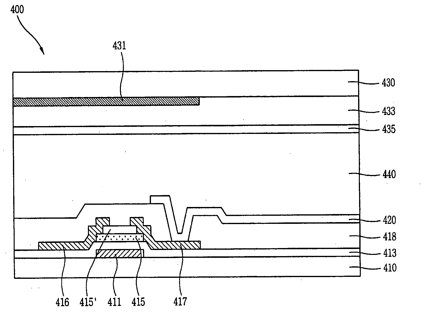
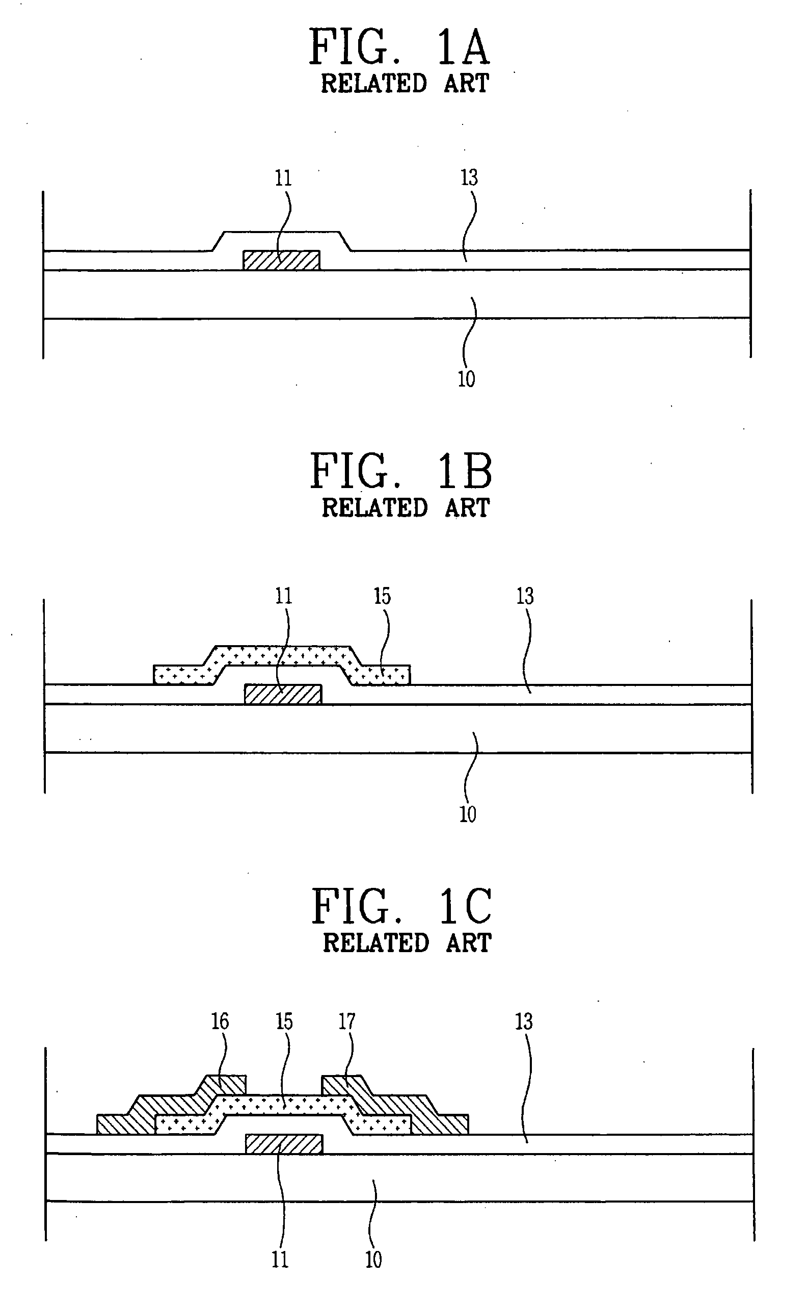
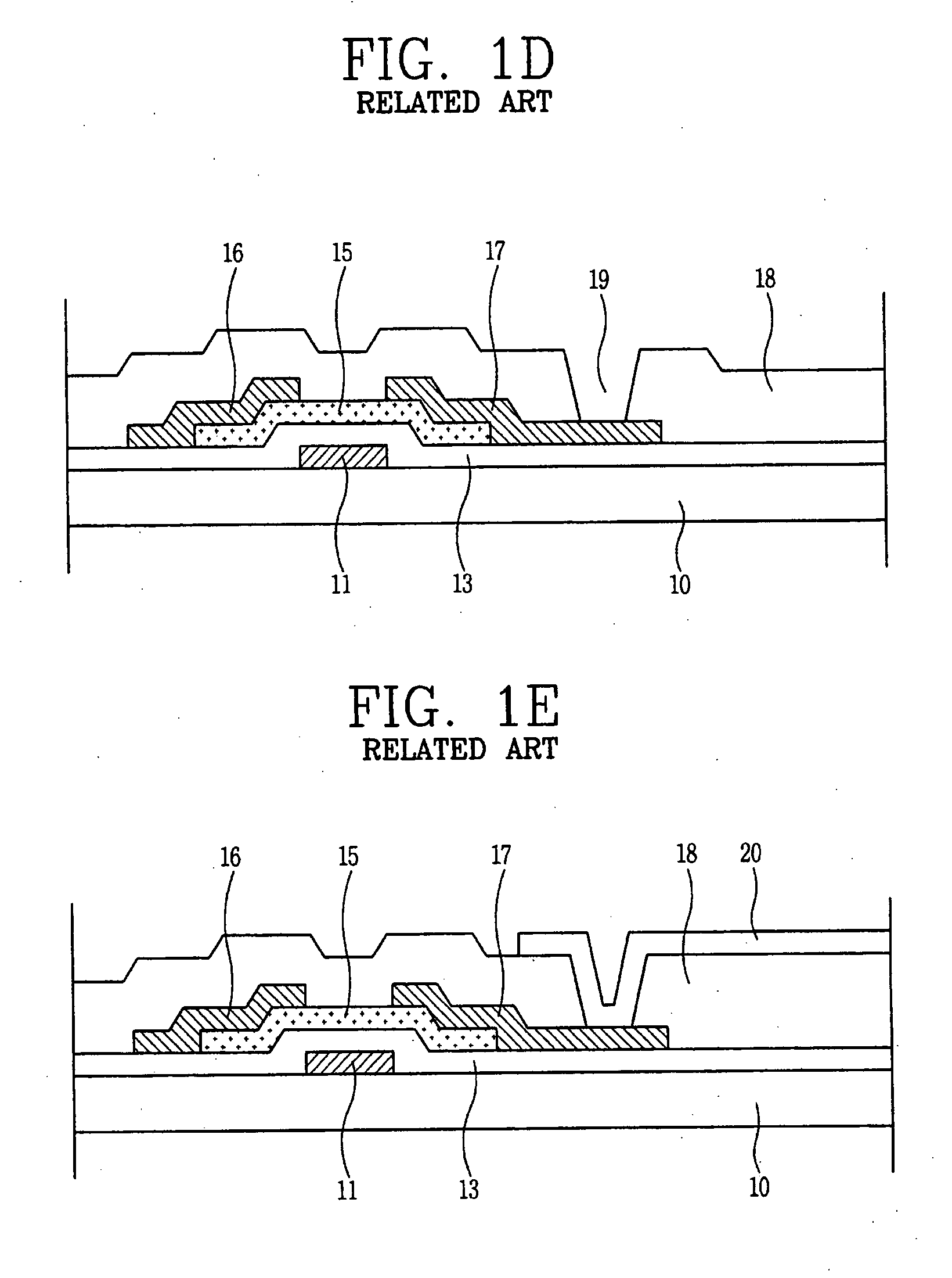
[0033]FIGS. 2A to 2E are cross-sectional views showing a method for fabricating an OTFT in accordance to an embodiment of the present invention, and FIGS. 3A to 3C are cross-sectional views showing a method for forming the active layer of the OTFT shown in FIG. 2B. As shown in FIG. 2A, a method for fabricating an OTFT includes preparing a first transparent substrate 110. In particular, a first conductive material is deposited and patterned to form a gate electrode 111.

[0034] The first conductive material may include one of Cu, Ti, Cr, Al, Mo, Ta and Al alloy, and the first conductive material may be patterned using a photolithography process. The photolithography process may include a photoresist film coating process for coating a photoresist film on an etching object layer on which a pattern is to be formed, an exposing ...


PUM


Abstract

A method for fabricating an organic thin film transistor includes forming a gate electrode on a substrate, forming a gate insulating layer on the substrate including the gate electrode, forming an organic active pattern on the gate insulating layer using a rear exposing process, and forming source and drain electrodes on the organic active pattern.

Description

[0001] The present invention claims the benefit of Korean Patent Application No. 68693 / 2004 filed in Korea on Aug. 30, 2004, and Korean Patent Application No. 68694 / 2004 filed in Korea on Aug. 30, 2004, which are hereby incorporated by reference. BACKGROUND OF THE INVENTION [0002] 1. Field of the Invention [0003] The present invention relates to a method for fabricating an organic thin film transistor, and more particularly, to a method for fabricating an organic thin film transistor and a method for fabricating a liquid crystal display device using the same that employ an rear exposing process to form an active layer. [0004] 2. Discussion of the Related Art [0005] Following the development of polyacetylene, which is a conjugated organic polymer exhibiting semiconductor characteristics, an organic semiconductor has been actively studied because its advantageous characteristics of easiness in formation of a film type, flexibility, conductivity and a low production cost. An organic se...

Claims


Application Information

Patent Timeline
Patent Type & Authority Applications(United States)
IPC IPC(8): H01L21/00H01L21/84H01L51/00H01L51/05H01L51/30
CPCG02F1/1368H01L51/0017H01L51/0018H01L51/0052H01L51/107H01L51/052H01L51/0525H01L51/0545H01L51/0516H10K71/231H10K71/233H10K85/615H10K10/468H10K10/472H10K10/471H10K10/88H10K10/466G02F1/136H10K59/10
Inventor SEO, HYUN-SIKNAM, DAE-HYUNCHOI, NACK-BONG
Owner LG DISPLAY CO LTD
Why Eureka
Try Eureka