Mask blank transparent substrate manufacturing method, mask blank manufacturing method, and exposure mask manufacturing method

a technology of transparent substrate and manufacturing method, applied in the direction of photomechanical equipment, instruments, originals for photomechanical treatment, etc., can solve the problems of reducing the transfer accuracy, the mask blank may not meet the specifications, and the flatness cannot be accurately estimated, so as to reduce the generation of mask blank defects, reduce the film stress of the thin film, and reduce the effect of film stress

Active Publication Date: 2006-08-31
HOYA CORP
View PDF4 Cites 20 Cited by
  • Summary
  • Abstract
  • Description
  • Claims
  • Application Information

AI Technical Summary

Benefits of technology

[0050] Further, the thin film forming step that forms the thin film on the transparent substrate (mask blank transparent substrate) is carried out after the surface shape information obtaining step, the simulation step, and the flatness calculation step. As a consequence, particles do not adhere to the thin film in those steps. Therefore, it is possible to suppress generation of defects on the mask blank to be manufactured.
[0051] According to the invention of the third or sixth aspect, the following effect can be achieved. The predetermined region of the main surface for obtaining the surface shape information in the surface shape information obtaining step is the region excluding the peripheral region of more than 0 mm and no more than 3 mm from the chamfered surface of the transparent substrate. As a consequence, the surface shape information in this predetermined region can be measured with high accuracy.
[0052] According to the invention of the seventh or eighth aspect, the following effect can be achieved. The film stress control step for reducing the film stress of the thin film is carried out at the time of and / or after carrying out the thin film forming step. Therefore, even when the film stress that deforms the transparent substrate (mask blank transparent substrate) is present in the thin film formed on the transparent substrate, this film stress can be reduced. As a result, it is possible to make consistency between the flatness of the transparent substrate which is calculated from the height information at the plurality of measurement points obtained by simulating the state where the transparent substrate is set in the exposure apparatus, and the flatness of the exposure mask obtained when the mask blank is manufactured by forming the thin film on the transparent substrate (mask blank transparent substrate), then the exposure mask is manufactured from this mask blank, and then this exposure mask is actually set in the exposure apparatus.
[0053] According to the invention of the ninth aspect, the following effect can be achieved. The surface shape of the main surface of the transparent substrate on the side where the thin film is formed is the shape such that the height of the main surface is gradually lowered from its center region to its peripheral portion. Therefore, when the exposure mask manufactured from the transparent substrate (mask blank transparent substrate) having such a shape is set in the exposure apparatus, the flatness of the exposure mask becomes excellent. Accordingly, it is possible to satisfy the specification required for the exposure mask.
[0054] According to the invention of the tenth aspect, the following effect can be achieved. The exposure mask is manufactured by patterning the thin film in the mask blank so as to form the thin film pattern on the transparent substrate (mask blank transparent substrate). Therefore, this exposure mask can satisfy the specification with respect to flatness, pattern position accuracy, and so on when it is set in the exposure apparatus. Accordingly, upon performing pattern transfer by the use of such an exposure mask, it is possible to improve the transfer accuracy.
[0055] According to the invention of the eleventh aspect, the following effect can be achieved. By the use of the exposure mask excellent in flatness and pattern position accuracy when it is set in the exposure apparatus, pattern transfer can be carried out onto a resist film formed on the substrate. Therefore, it is possible to manufacture the semiconductor apparatus with an accurate pattern exactly as designed and free from a pattern defect.

Problems solved by technology

In this manner, transfer accuracy is often reduced.
After a mask blank is produced by forming a light-shielding film on a transparent substrate, if the flatness and the surface shape of this mask blank are measured, quite a large number of particles adhere to the light-shielding film to cause defects.
As a consequence, the mask blank may not satisfy those specifications.
Accordingly, there is a possibility that the flatness cannot be accurately estimated.

Method used


Image

  • Mask blank transparent substrate manufacturing method, mask blank manufacturing method, and exposure mask manufacturing method
  • Mask blank transparent substrate manufacturing method, mask blank manufacturing method, and exposure mask manufacturing method
  • Mask blank transparent substrate manufacturing method, mask blank manufacturing method, and exposure mask manufacturing method

Examples


example

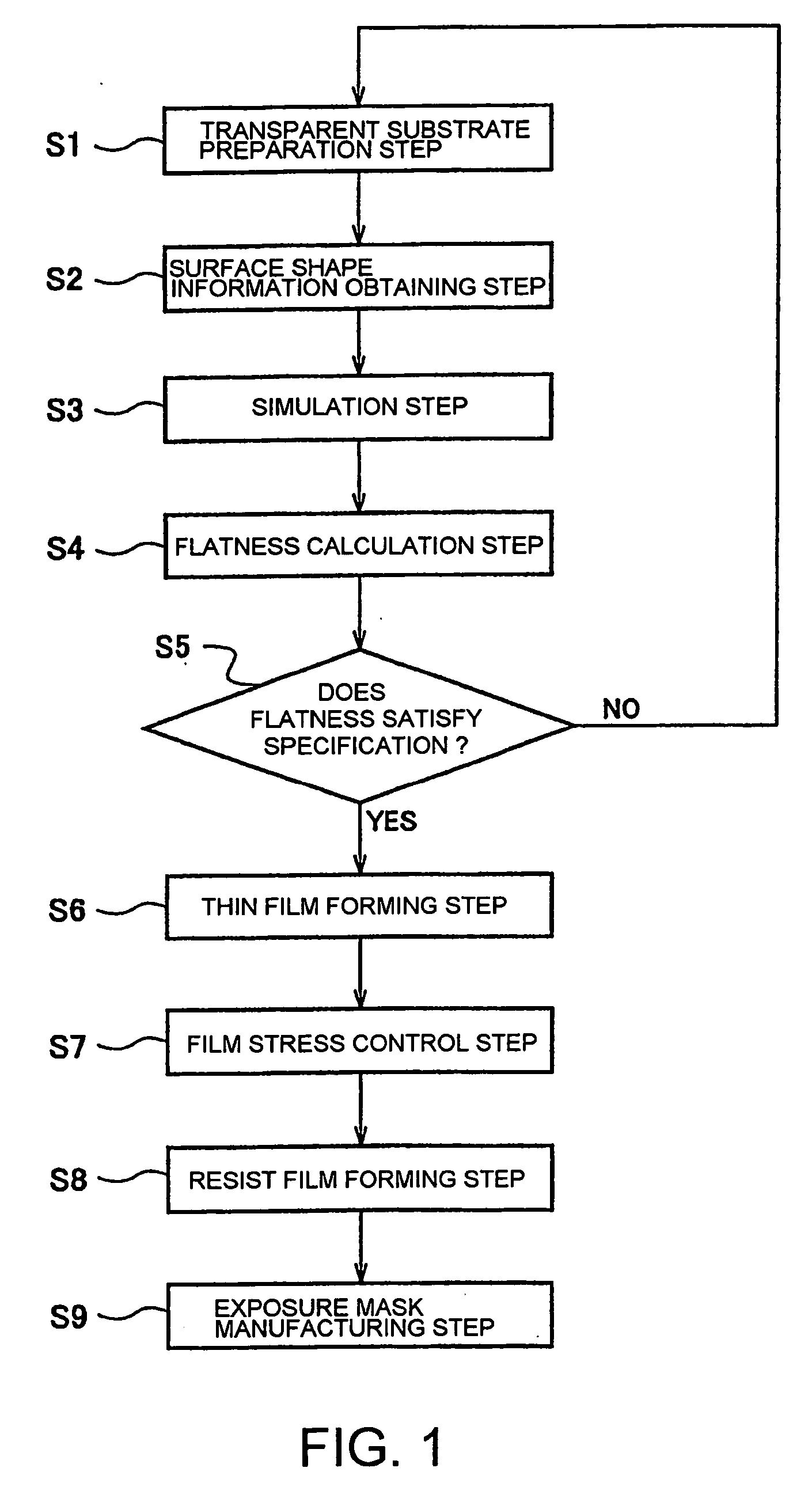
[0105] Hereinbelow, description will be made in detail about steps of manufacturing a halftone phase shift mask blank as a mask blank.

[0106] (I) Transparent Substrate Preparation Step

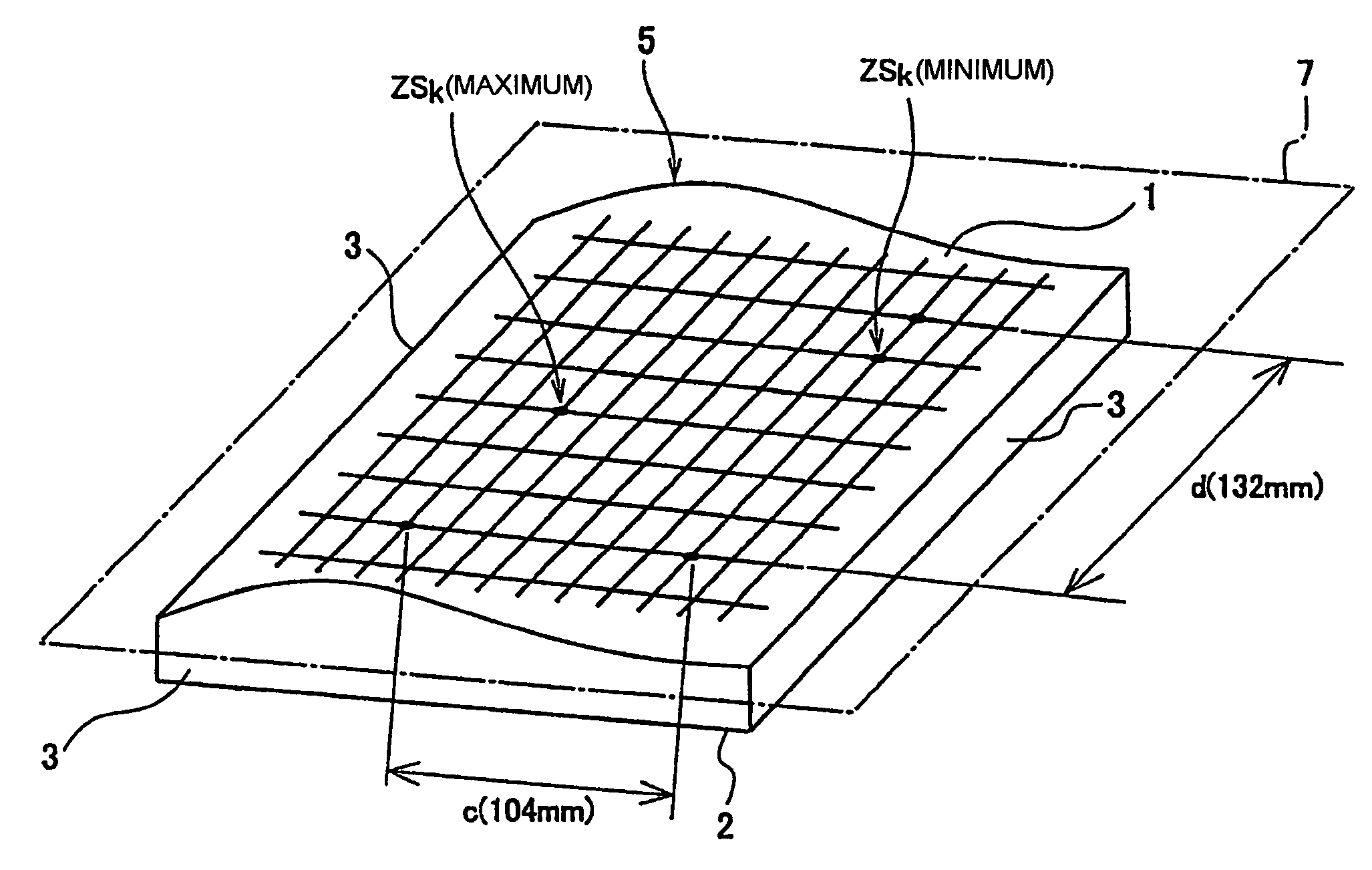
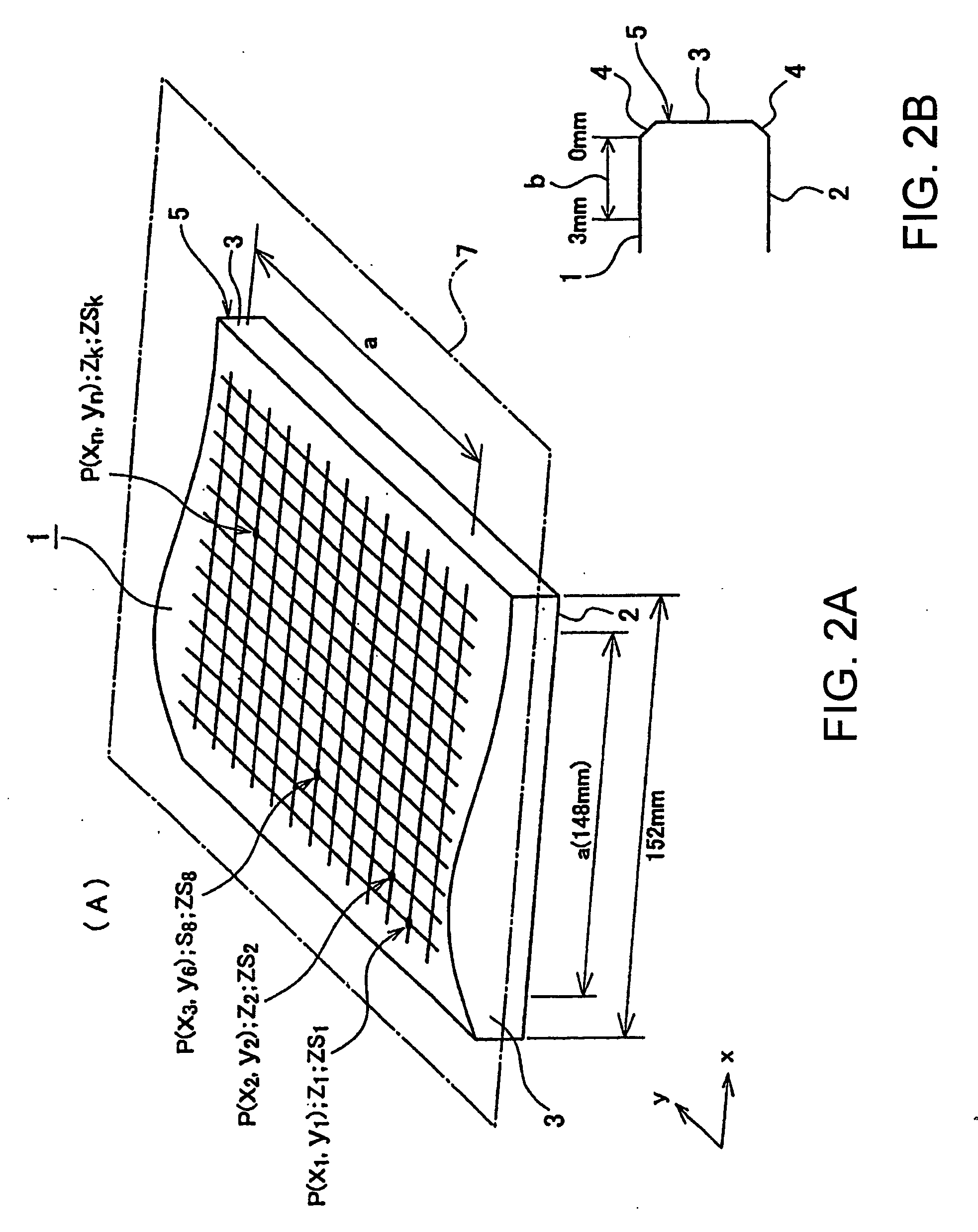
[0107] Main surfaces of a square transparent plate (synthetic quartz glass plate) having a size of 152 mm×152 mm were precision-polished and cleaned. Thus, a transparent substrate was prepared.

[0108] (II) Surface Shape Information Obtaining Step

[0109] By the use of a flatness measuring apparatus (UltraFlat200M manufactured by Corning Tropel) utilizing an optical interferometer, surface shape information (height information from a focal plane (virtual absolute plane) calculated by the method of least squares) was obtained at 256×256 measurement points in a predetermined region (148 mm×148 mm) on the main surface (the main surface where a thin film was going to be formed) of the transparent substrate and stored in a computer. According to this surface shape information, the surface shape of the main s...


PUM

PropertyMeasurementUnit
wavelengthaaaaaaaaaa
exposure wavelengthaaaaaaaaaa

Abstract

A method includes a preparation step of preparing a transparent substrate having a precision-polished main surface, a surface shape information obtaining step of obtaining, as surface shape information, height information at a plurality of measurement points on the main surface of the transparent substrate that contacts a mask stage of an exposure apparatus, a simulation step of obtaining, based on the surface shape information and shape information of the mask stage, height information at the plurality of measurement points by simulating the state where the transparent substrate is set in the exposure apparatus, a flatness calculation step of calculating, based on the height information obtained through the simulation, a flatness of the transparent substrate when it is set in the exposure apparatus, a judging step of judging whether or not the calculated flatness satisfies a specification, and a thin film forming step of forming a thin film as serving as a mask pattern, on the main surface of the transparent substrate whose flatness satisfies the specification.

Description

[0001] This invention claims priority to prior Japanese patent application JP 2005-50936, the disclosure of which is incorporated herein by reference. BACKGROUND OF THE INVENTION [0002] This invention relates to a method of manufacturing a transparent substrate for a mask blank suitable for a short wavelength region where the exposure wavelength is 200 nm or less, and further relates to a mask blank manufacturing method and an exposure mask manufacturing method. [0003] In recent years, following the miniaturization of semiconductor devices, exposure light sources used in the photolithography technique have been changing to an ArF excimer laser (exposure wavelength: 193 nm) and an F2 excimer laser (exposure wavelength: 157 nm) so that reduction in exposure wavelength has been proceeding. [0004] When the exposure wavelength becomes 200 nm or less, the depth of focus of an exposure apparatus becomes extremely small. Accordingly, if an exposure mask is deformed to reduce its flatness wh...

Claims


Application Information

Patent Timeline
Patent Type & Authority Applications(United States)
IPC IPC(8): B32B9/00G03C5/00B32B17/06G03F1/00G03F1/50G03F1/68H01L21/027
CPCG03F1/60G03F7/705G03F7/70783G03F1/14G03F1/32G03F7/70483G03F1/62
Inventor TANABE, MASARU
Owner HOYA CORP
Why Eureka
Try Eureka