Pattern forming method and phase shift mask manufacturing method

a technology of mask manufacturing and pattern forming, applied in the field of pattern forming method, can solve the problems of increasing the number of figures to be written, long time is also required for writing on resist film, and increasing the amount of data to be processed, so as to suppress the occurrence of defects, reduce the amount of pattern data, and achieve accurate and efficient fabrication.

Active Publication Date: 2007-08-16
HOYA CORP
View PDF8 Cites 18 Cited by
  • Summary
  • Abstract
  • Description
  • Claims
  • Application Information

AI Technical Summary

Benefits of technology

[0029]In this invention, the writing data to be used in writing on the resist film formed on the coating layer (or the light-shielding layer) includes a portion where pattern data corresponding to at least two recesses adjacent to each other through a remaining portion in the coating layer (or through a light-shielding portion in a light-shielding pattern) are combined into one pattern data and, therefore, the pattern data amount can be reduced. Further, since it is possible to suppress occurrence of a defect that depends on a pattern layout, fabrication can be carried out accurately and efficiently.
[0030]That is, this invention can achieve a reduction in writing data amount in a manufacturing method of a phase shift mask such as an auxiliary pattern type phase shift mask. Further, according to the manufacturing method of this invention, it is possible to suppress occurrence of a defect that depends on a pattern layout, thereby manufacturing the phase shift mask accurately and efficiently.
[0031]This invention can achieve a reduction in writing data amount even when applied to a pattern forming method adapted to process a coating layer over a substrate into a predetermined pattern by partly removing the coating layer and then form recesses in an underlying layer below the coating layer [at at least a part of where the coating layer is removed. Further, according to this pattern forming method, it is possible to suppress occurrence of a defect that depends on a pattern layout, thereby carrying out pattern formation accurately and efficiently.

Problems solved by technology

When the pattern data amount increases, a long time is required for data processing and, further, a long time is also required for writing on a resist film.
Particularly, in recent years, since the electron-beam writing method has shifted from the raster scan type to the vector scan type for improving the pattern accuracy, an increase in pattern data amount directly leads to an increase in the number of figures to be written, thus directly leading to an increase in writing time.
Further, since an auxiliary opening pattern that is not resolved on a substrate to which a pattern is transferred is arranged around a main opening portion (contact hole), there arises a problem in mask fabrication due to limitation to a layout manner or occurrence of an irregular layout depending on design of an LSI.
If, in this manner, the part of the resist pattern 110 falls down to close the opening portion, a transparent substrate 101 is not etched at the closed portion as shown in FIGS. 4D and 4E, resulting in occurrence of a defect.

Method used


Image

  • Pattern forming method and phase shift mask manufacturing method
  • Pattern forming method and phase shift mask manufacturing method
  • Pattern forming method and phase shift mask manufacturing method

Examples


first embodiment

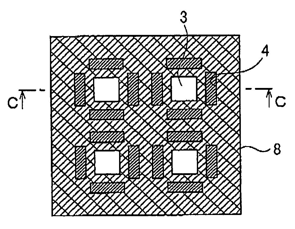
[0047]FIGS. 5A and 5B are plan views for explaining a structure of a phase shift mask manufactured by a first embodiment of a phase shift mask manufacturing method according to this invention.

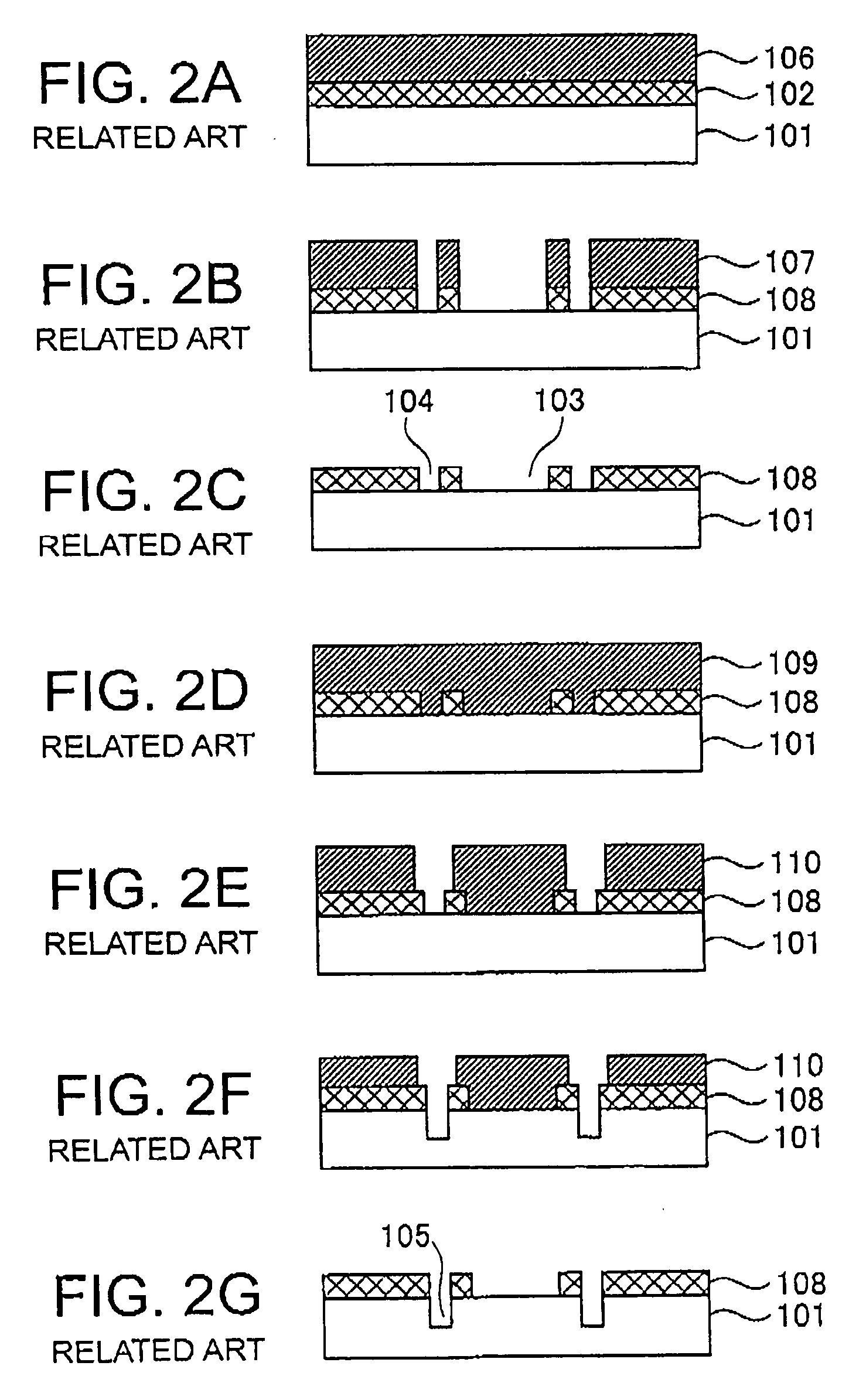
[0048]FIGS. 6A to 6G are process diagrams showing the first embodiment of the phase shift mask manufacturing method according to this invention.

[0049]In the first embodiment, a description will be given of the case of manufacturing an auxiliary pattern type phase shift mask in which four main opening portions 3 are arranged in two rows and two columns as shown in FIG. 5A. Four auxiliary opening portions 4 are arranged around each main opening portion 3. In this case, there exist four pairs each including the two auxiliary opening portions 4 with their long sides adjacent to each other.

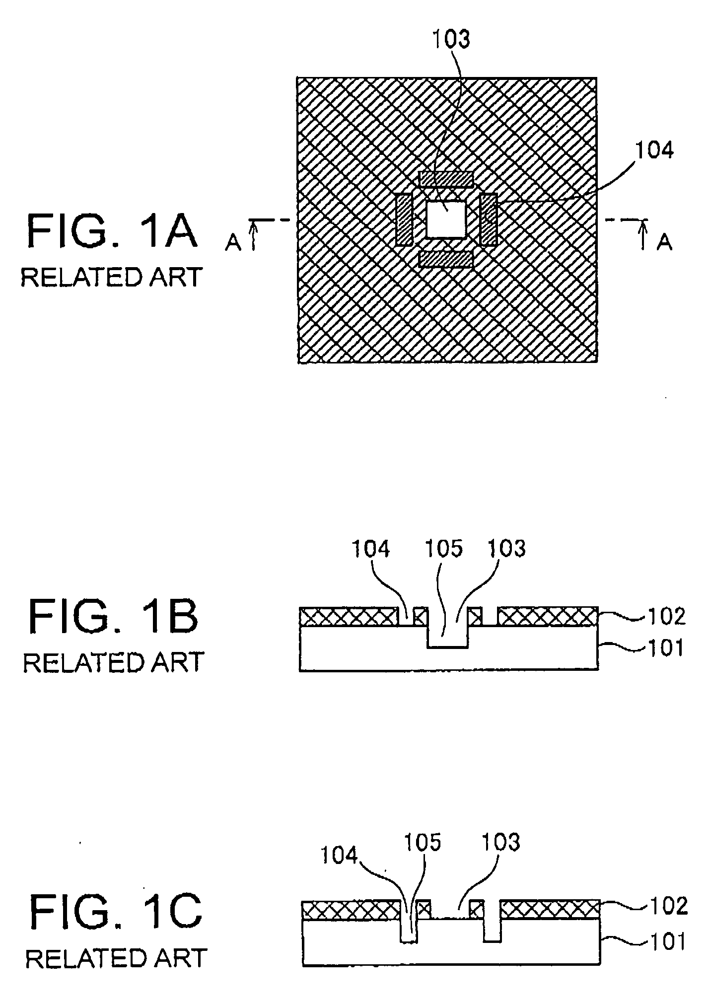
[0050]In the phase shift mask manufacturing method according to the first embodiment, in order to manufacture an auxiliary pattern type phase shift mask, a light-shielding layer (or a coating layer) 2 and a first ...

second embodiment

[0062]FIGS. 10A and 10B are a sectional view and a plan view, respectively, showing a second embodiment of a phase shift mask manufacturing method according to this invention.

[0063]In the first embodiment, the positive-type resist is used when forming the second resist pattern 10. However, a negative-type resist may also be used in the phase shift mask manufacturing method according to this invention.

[0064]Therefore, in the second embodiment, a negative-type resist is used as the second resist film 9 in FIG. 6D in the first embodiment and, as shown in FIG. 10B, pattern data corresponding to the main opening portions 3 are used as writing data for forming a second resist pattern 10 instead of the pattern data corresponding to the auxiliary opening portions 4. In the case where the negative-type resist is used as the second resist film 9, the second resist film 9 is left remaining by writing in the regions of the main opening portions 3 where the etched portions 5 are not formed, whil...

first example

[0068]Hereinbelow, a description will be given of a first example of a phase shift mask manufacturing method according to this invention.

[0069]As a transparent substrate, there was prepared a quarts glass substrate having mirror-polished surfaces and subjected to predetermined cleaning. This transparent substrate had a 6-inch square size with a thickness of 0.25 inches. At first, a light-shielding layer made of chromium and having a thickness of 100 nm was formed on the transparent substrate by sputtering. Then, as a first resist film, a positive-type electron-beam resist (“ZEP7000” manufactured by Zeon Corporation) was coated to a thickness of 400 nm on the light-shielding layer by spin coating.

[0070]Then, the first resist film was written with a pattern corresponding to a main opening portion and auxiliary opening portions by the use of an electron-beam writing apparatus and then developed, thereby forming a first resist pattern. Then, dry etching using a mixed gas of Cl2 and O2 w...


PUM

PropertyMeasurementUnit
thicknessaaaaaaaaaa
thicknessaaaaaaaaaa
thicknessaaaaaaaaaa

Abstract

A phase shift mask manufacturing method comprises the steps of processing a light-shielding layer over a transparent substrate into a predetermined light-shielding pattern, forming a resist film on the predetermined light-shielding pattern, performing writing on the resist film based on writing data and developing the resist film, thereby forming a resist pattern, and etching an underlying layer using the predetermined light-shielding pattern and the resist pattern as a mask, thereby forming recesses, that serve as phase shift portions, in the underlying layer. The writing data includes a portion where pattern data corresponding to at least the two recesses adjacent to each other through a light-shielding portion in the predetermined light-shielding pattern are combined into one pattern data.

Description

[0001]This application claims priority to prior Japanese application JP 2006-39220, the disclosure of which is incorporated herein by reference.BACKGROUND OF THE INVENTION[0002]This invention relates to a pattern forming method and, in particular, relates to a pattern forming method that processes a coating layer over a substrate into a predetermined pattern by partly removing the coating layer and then forms a recess in an underlying layer below the coating layer at its portion corresponding to at least a portion of a region where the coating layer is removed.[0003]This invention also relates to a method of manufacturing a phase shift mask for use in transferring a fine pattern of an LSI or the like by the use of a projection exposure apparatus.[0004]Following higher integration and circuit pattern miniaturization in large-scale integrated circuits (LSIs), phase shift masks have been proposed and put to practical use as a super-resolution technique in the photolithography.[0005]The...

Claims


Application Information

Patent Timeline
Patent Type & Authority Applications(United States)
IPC IPC(8): G03C5/00G03F1/00G03F1/29G03F1/68H01L21/027
CPCG03F1/144G03F1/32G03F1/30G03F1/29G03F1/36G03F1/80
Inventor SUDA, HIDEKI
Owner HOYA CORP
Why Eureka
Try Eureka