Semiconductor device with bumps on electrode pads oriented in given direction

Inactive Publication Date: 2005-08-23
SHARP KK
View PDF26 Cites 18 Cited by
  • Summary
  • Abstract
  • Description
  • Claims
  • Application Information

AI Technical Summary

Benefits of technology

[0020]It is an object of the present invention to provide a semiconductor device which suppresses an occurrence of a defect such as a bump defect, etc., and enables a narrowing of an electrode pad pitch.
[0022]According to the described arrangement, as a plurality of divided bump electrodes are provided for each electrode pad, compared with the case of adopting a single bump electrode, an occurrence of a defective bump electrode can be suppressed. Namely, in the case of a single bump electrode, if a bump defect occurs, or a significant gap is generated between heights of the adjoining bump electrodes, etc., a connection inferior occurs when mounting the semiconductor device. However, in the case of adopting a plurality of divided bump electrodes, even if a bump defect or a gap between heights of the adjoining bump electrodes occurs in some of the plurality of divided bump electrodes, as long as at least one bump electrode is connected, an occurrence of the connection inferior can be avoided. As the described arrangement permits a significantly lower proportion of a connection inferior when mounting the semiconductor device, an improved yield in manufacturing the bump electrodes and an improved reliability of a connected state can be achieved.
[0023]Furthermore, as the plurality of bump electrodes are aligned in a direction orthogonal to the direction where the electrode pads are aligned, an interval between the electrode pads can be reduced to the minimum. As this permits a narrower electrode pad pitch, the size of a semiconductor device can be reduced.
[0024]It is another object of the present invention to provide a manufacturing method of a semiconductor device of the present invention which permits bump electrodes to be prepared at a significantly improved yield.
[0027]According the described method, mutual effects among the plurality of bump electrodes when plating can be eliminated, thereby achieving a significantly improved yield of the bump electrodes.
[0031]In order to counteract the described problems, the method of testing the semiconductor device in accordance with the present invention is arranged such that the test prober is made in contact with the bump electrode formed on the inner most side. As a result, even in an event of an abnormality in an applied pressure to a probe needle, the defective bump in its shape due to a mechanical strength applied when testing using the test prober can be suppressed to the minimum.

Problems solved by technology

Namely, in the case of a single bump electrode, if a bump defect occurs, or a significant gap is generated between heights of the adjoining bump electrodes, etc., a connection inferior occurs when mounting the semiconductor device.
However, in the case of adopting a plurality of divided bump electrodes, even if a bump defect or a gap between heights of the adjoining bump electrodes occurs in some of the plurality of divided bump electrodes, as long as at least one bump electrode is connected, an occurrence of the connection inferior can be avoided.

Method used


Image

  • Semiconductor device with bumps on electrode pads oriented in given direction
  • Semiconductor device with bumps on electrode pads oriented in given direction
  • Semiconductor device with bumps on electrode pads oriented in given direction

Examples


Embodiment Construction

[0054]The following descriptions will explain one embodiment of the present invention in reference to FIG. 1 through FIG. 12. In the present embodiment, explanations will be given through the case of a liquid crystal display device wherein a semiconductor chip as a semiconductor device is mounted by the ACF-COG method.

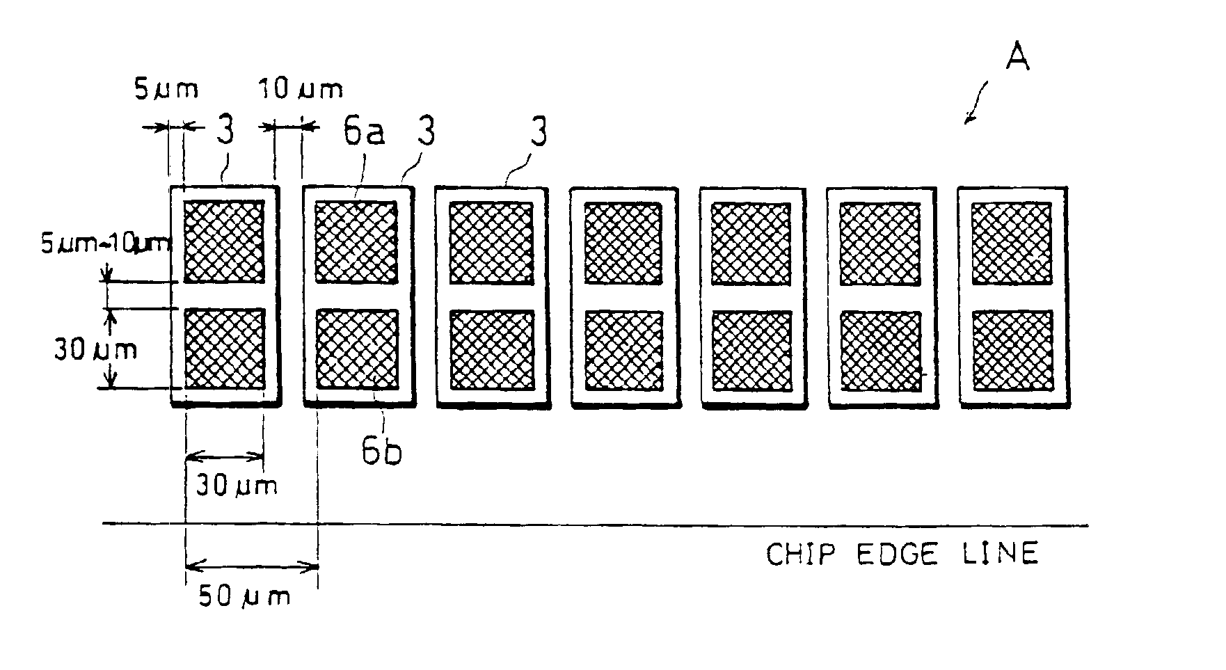
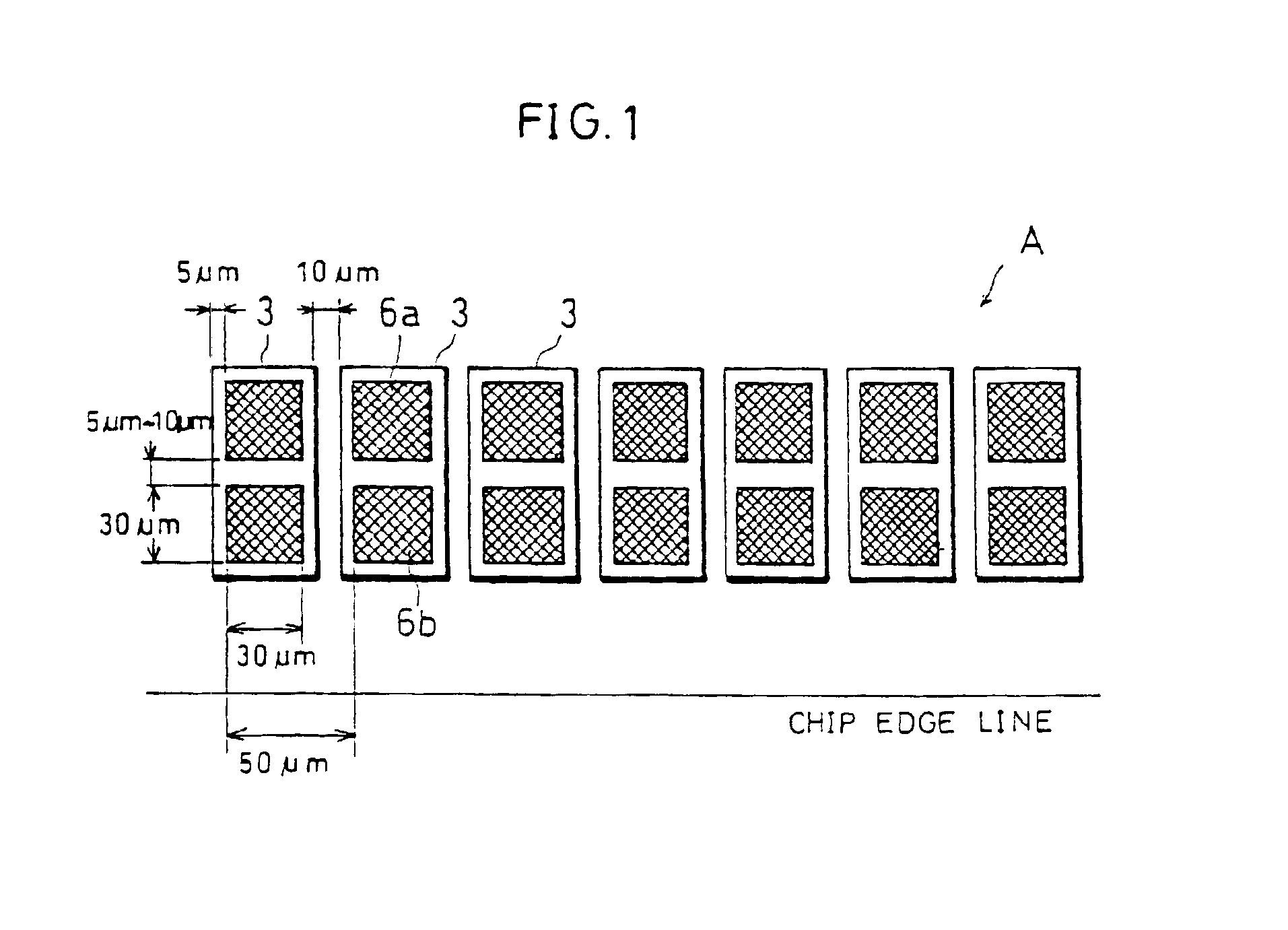
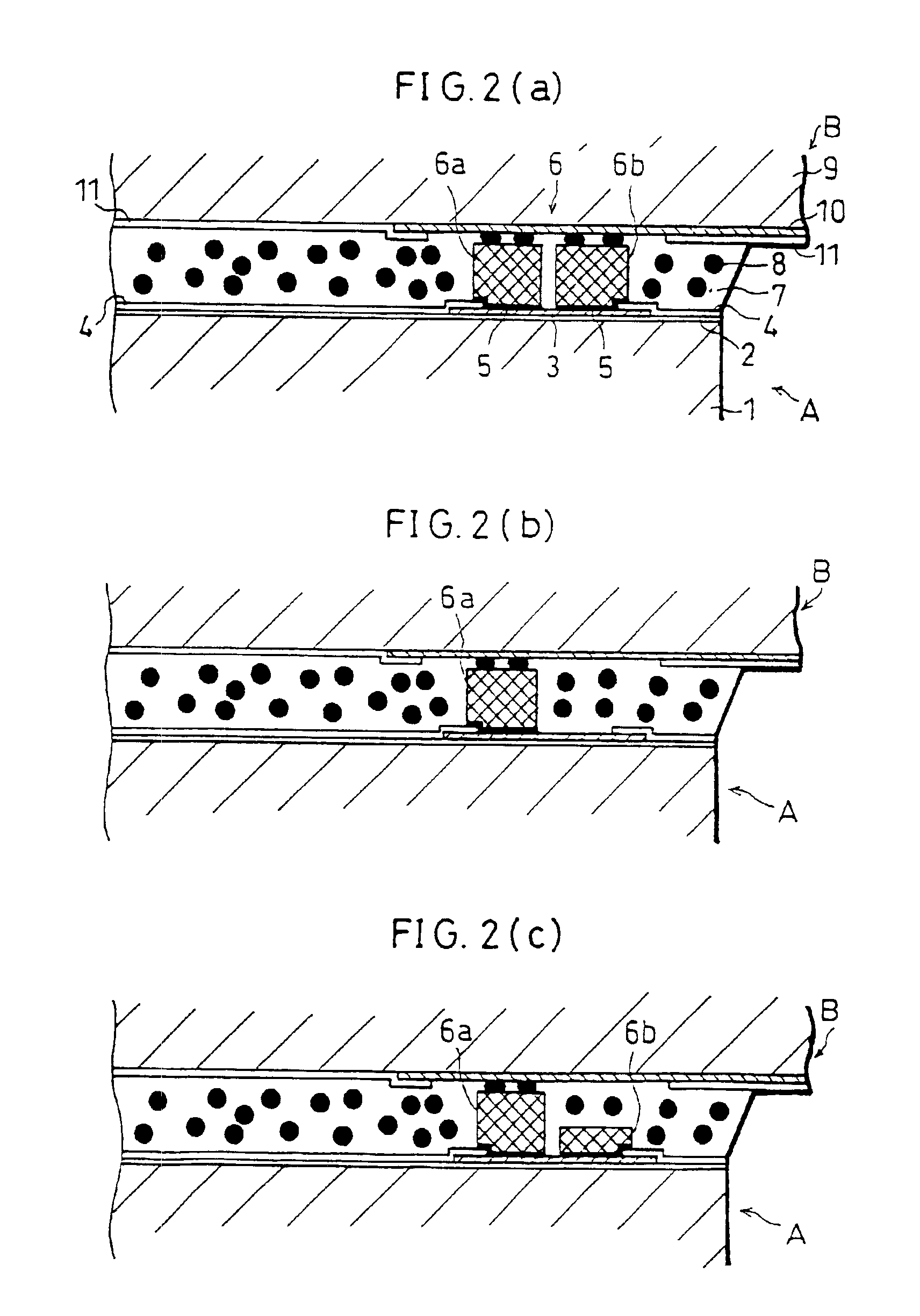
[0055]FIG. 2(a) is a cross-sectional view showing a part of the liquid crystal display device where the semiconductor chip is mounted. As shown in FIG. 2(a), a semiconductor chip A includes a semiconductor substrate 1 whereon an insulating film 2, an electrode pad 3, and an opening section 4a (see FIG. 3(b)) are formed in this order. Further, a bump electrode 6 is formed on the opening section 4a via a barrier metal 5. The opening section 4a has a slightly smaller diameter than the circumference of the bump electrode 6. The bump electrode 6 is composed of two bump electrodes 6a and 6b which are provided on the inner side and the edge side of the semiconductor chip A re...


PUM


Abstract

A semiconductor device includes a semiconductor substrate, a plurality of electrode pads aligned on the semiconductor substrate, and a plurality of bump electrodes placed on each electrode pad, wherein the plurality of bump electrodes on the electrode pad are aligned in a direction orthogonal to a direction where the electrode pads are aligned. A manufacturing method of the semiconductor device includes the steps of patterning a photoresist which serves as a bump electrode forming use mask on the semiconductor substrate having formed thereon the electrode pads and forming a bump electrode in a perpendicular straight wall shape to be thinner than the photoresist by plating the bump electrode forming use metal to the electrode pad.

Description

[0001]This application is a division of application Ser. No. 08 / 989,328, filed Dec. 11, 1997 now U.S Pat. No. 6,525,422, the entire content of which is hereby incorporated by reference in this application.FIELD OF THE INVENTION[0002]The present invention relates to a semiconductor device including bump electrodes, a manufacturing method and a testing method of the same, and also relates to a liquid crystal display device, a circuit substrate and a tape carrier package (hereinafter referred to as TCP) respectively including the semiconductor device.BACKGROUND OF THE INVENTION[0003]Known methods of electrically connecting a semiconductor device to a liquid crystal display device, a circuit substrate or a TCP include a wireless bonding method wherein a bump electrode is provided on an electrode terminal of a semiconductor device, and the semiconductor device is bonded directly to the liquid crystal display device, the circuit substrate or the TCP using the bump electrode.[0004]A concre...

Claims


Application Information

Patent Timeline
IPC IPC(8): H01L23/485H01L23/48H01L21/60
CPCH01L24/10H01L24/13H01L2224/13099H01L2924/01004H01L2924/01013H01L2924/01015H01L2924/01022H01L2924/01033H01L2924/01074H01L2924/01078H01L2924/01079H01L2924/01082H01L2924/01322H01L2924/14H01L2924/01005H01L2924/01006H01L2924/01024H01L2924/014H01L2924/00H01L2224/05001H01L2224/05022H01L2224/05572H01L2224/13H01L2224/1411H01L2924/15787H01L2924/351H01L2224/05541H01L2224/05005H01L21/321H01L23/544H01L21/60
Inventor ONO, ATSUSHICHIKAWA, YASUNORIKANDA, MAKOTONIE, NORIMITSUTONE, SATORUSHIOTA, MOTOJIINOHARA, AKIOYOSHIDA, HIROKAZU
Owner SHARP KK
Why Eureka
Try Eureka