Method for manufacturing a contact for testing a semiconductor device

Inactive Publication Date: 2014-03-13
SILICONE VALLEY
View PDF2 Cites 0 Cited by
  • Summary
  • Abstract
  • Description
  • Claims
  • Application Information

AI Technical Summary

Benefits of technology

The present invention allows for the determination of the distance between adjacent electrical conductor parts based on the thickness of the layers and the width of the cut during manufacturing. This results in a narrower pitch between the conductor parts, as compared to related art methods that require a perforating process. The layers can be easily and precisely formed or cut without using high-technology methods, leading to a cost-effective and easy manufacturing process. The size and interval of the layers can be adjusted to form layers in a variety of forms with the desired thickness and width. The narrow pitch between conductor parts makes it easy to arrange semiconductor devices in close proximity to each other, and the separate stacking of the layers ensures reliable conductivity for accurate testing of the semiconductor device.

Problems solved by technology

In this method, however, the size of the perforation and the pitch between perforations cannot be physically made narrower than 250 μm, hundreds of thousands of perforations are required, so the time taken for forming the perforations is prolonged, and, during the perforating process or due to hundreds of thousands of perforations themselves, the dielectric plate becomes structurally weak, thereby being subjected to breakage, cracks, deformation, etc.
Thus, a contact manufactured using such a manufacturing method, or a die for manufacturing the contact has limits to properly form the size of the perforation or pitch of the perforations for forming a conductor portion, as well as it is difficult to manufacture the contact or the die.
Further, a high-tech micro milling machine is required in order to increase precision, so a manufacturing cost increases.
Furthermore, upon machining with the precision of 250 μm or less, even such a micro milling machine also has a high error rate due to a mechanical error during micro machining.
This method also has problems in that, because upper and lower dies, magnets, a pin for applying magnetic force, and the like essentially require perforations according to the above-mentioned machining method, there are limitations in narrowing a pitch.
Further, when the conductive pillars are magnetically formed, the movement of metal powders is not easy due to the viscosity of liquid, so that it is difficult to provide a vertical alignment, and there is a risk of adjacent conductive pillars being interlinked, causing an electrical connection error.
This method enables easy manufacture compared to the related art technology, but has a reduced reliability in the manufacture.

Method used


Image

  • Method for manufacturing a contact for testing a semiconductor device
  • Method for manufacturing a contact for testing a semiconductor device
  • Method for manufacturing a contact for testing a semiconductor device

Examples


Embodiment Construction

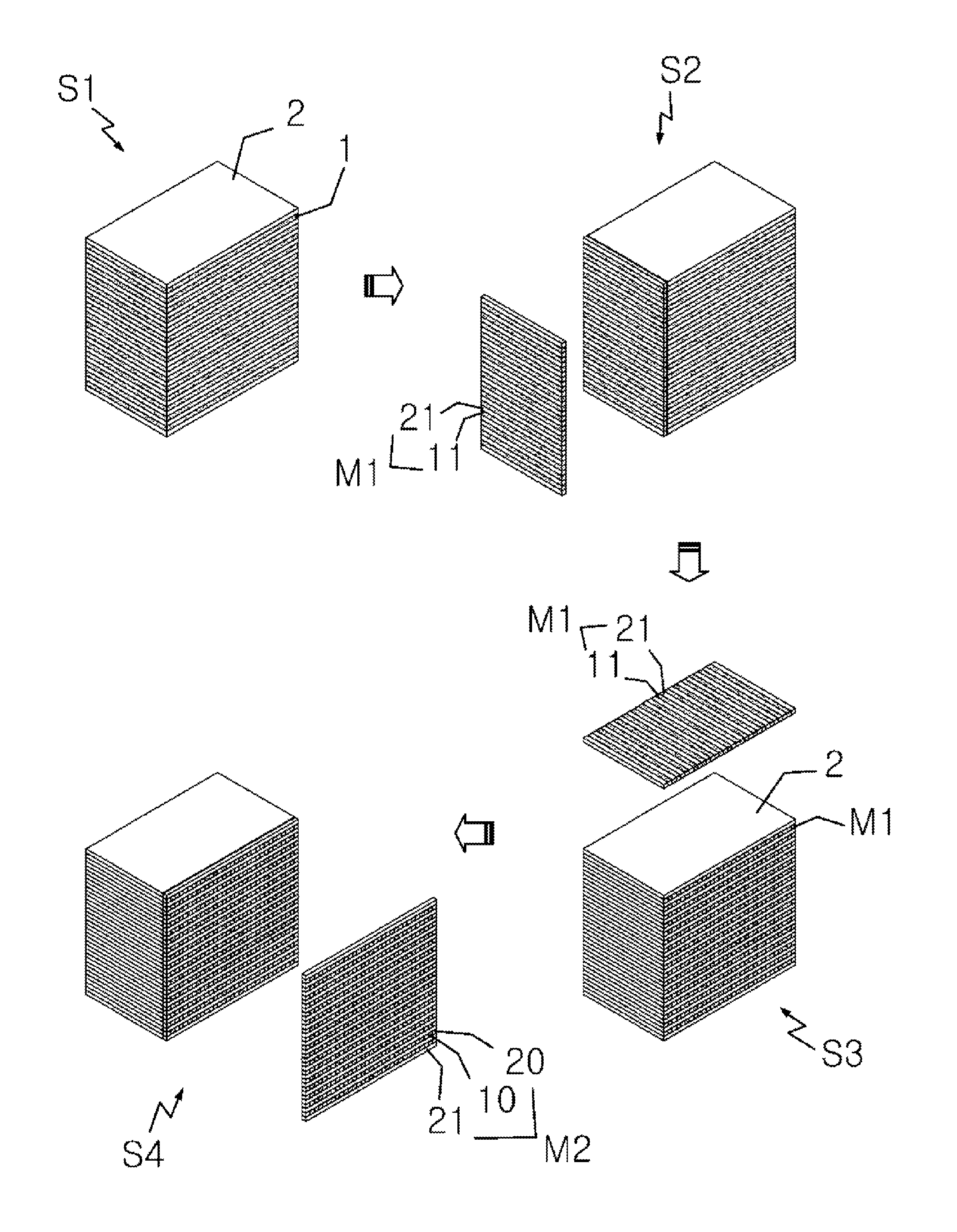
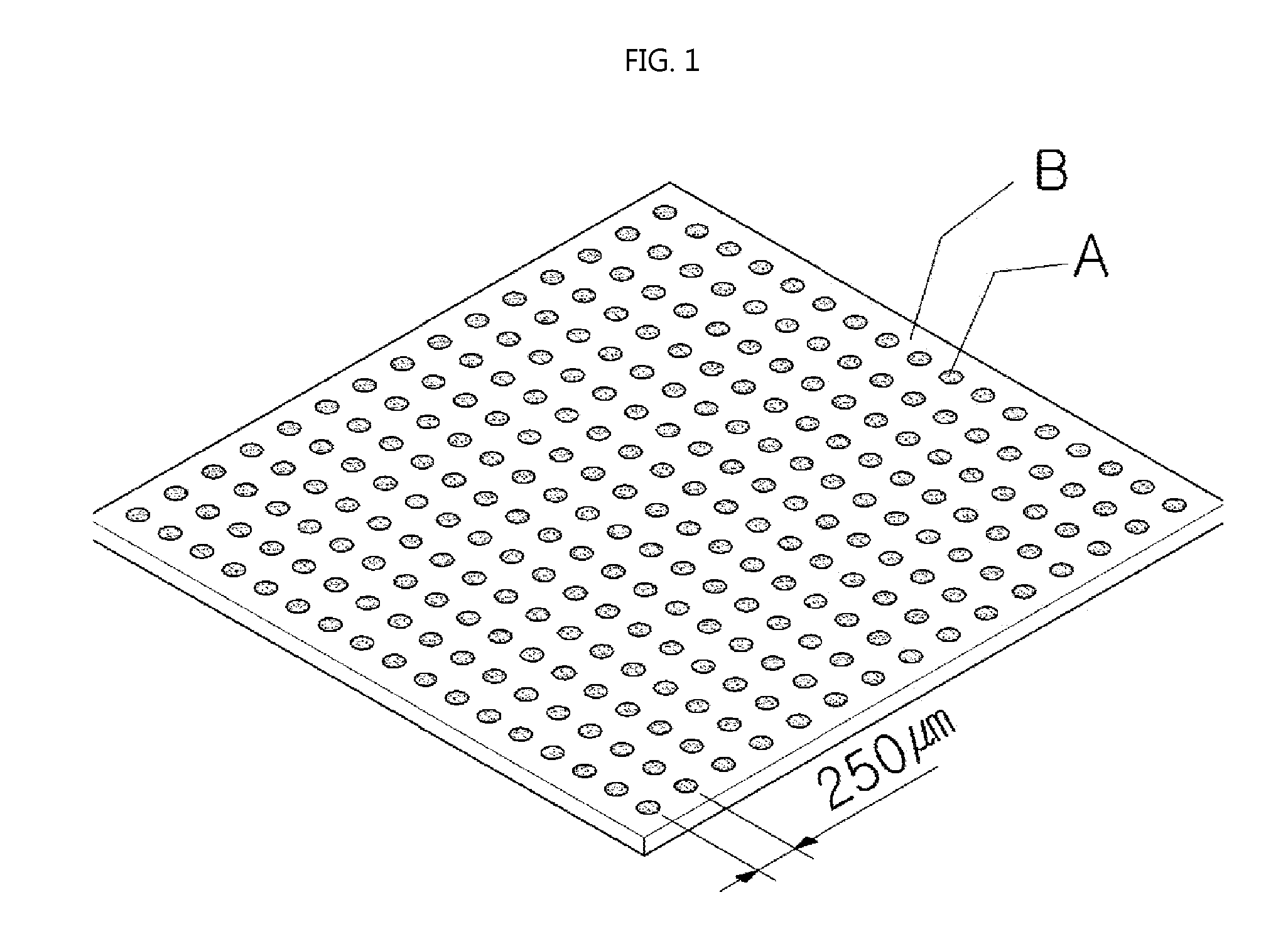
[0026]First, referring to a contact shown in FIG. 1 which is manufactured by a conventional method, the contact is configured so that a plurality of electrically conductive column-type portions A are uniformly arranged on an electrically nonconductive dielectric plate B.

[0027]As described before, this configuration is obtained by filling a perforated dielectric plate B with a conductive material, or as disclosed in the above-mentioned cited document, by providing conductive metal powders in a liquefied dielectric and magnetically forming conductive pillars.

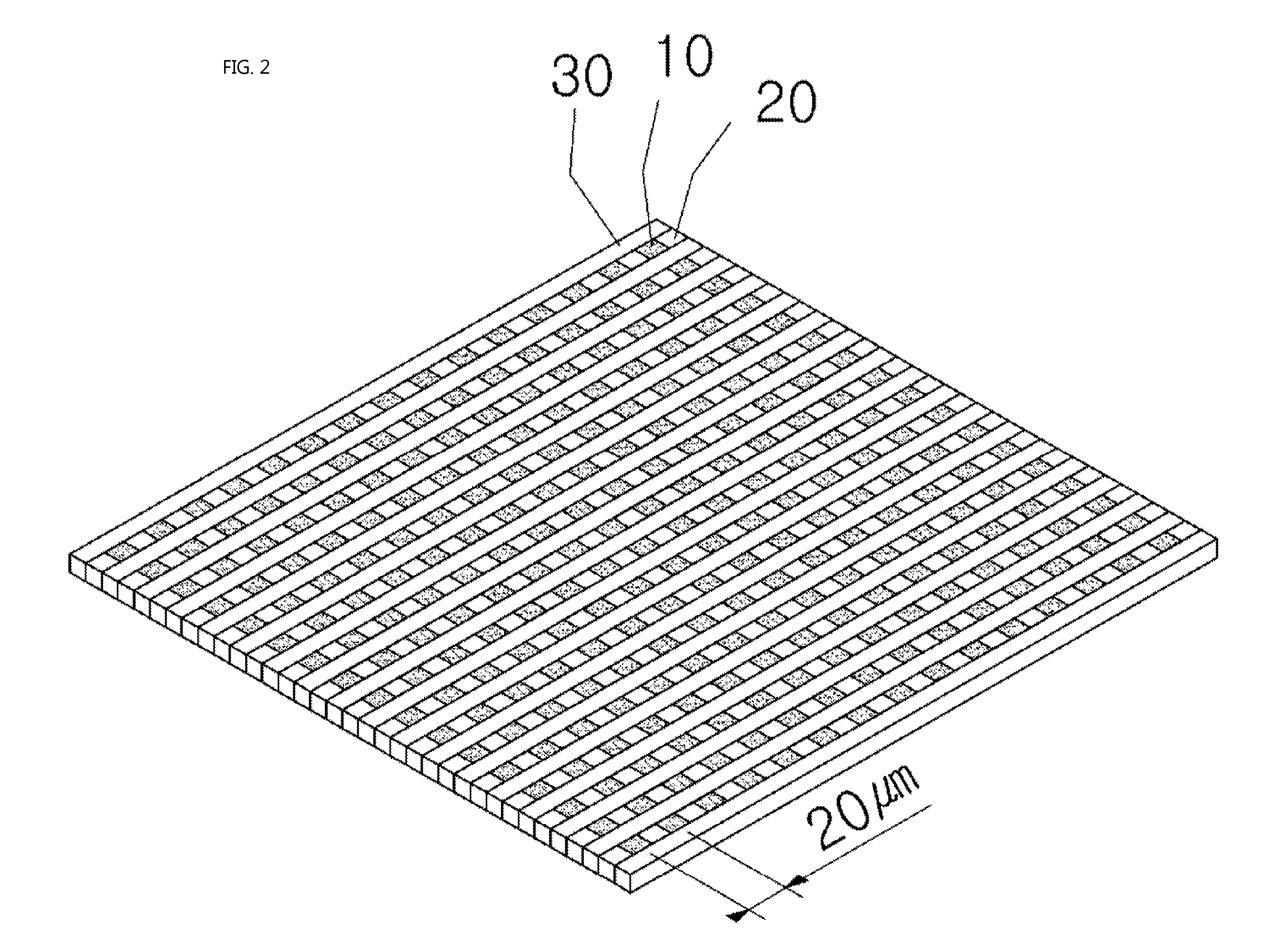
[0028]However, both the methods essentially require perforations, which are formed directly in the dielectric plate or in dies by a mechanical machining method, in order to fabricate a contact. Here, since a pitch of perforations formed by mechanical machining can be physically limited to 250 μm or more, in the case of micro semiconductor device, there are many limitations on contact, a position, a quantity, a disposition, etc.

[00...


PUM

PropertyMeasurementUnit
Thicknessaaaaaaaaaa
Widthaaaaaaaaaa

Abstract

The present invention relates to a contact for a test socket in which conductor portions are formed so as to be arranged at certain intervals on a dielectric plate used for testing whether a semiconductor device is normal by contacting a read terminal of the semiconductor device, and more particularly, to a method for manufacturing a contact for testing a semiconductor device, wherein a dielectric plate and a conductor portion are continuously alternately bonded and stacked repeatedly, one side of the stack is cut, then the stack and a dielectric layer are again subjected to repeated alternating bonding and stacking, after which the front surface of the stack is cut to yield a finished product of a new type of contact. Thus, the pitch between adjacent conductor portions can be determined according to the thickness at which layers are formed and the cut width in the manufacturing process, so that a desired pitch of the conductor portion can be achieved.

Description

TECHNICAL FIELD [0001]The present invention relates to a contact for a test socket in which conductor portions are formed so as to be arranged at certain intervals on a dielectric plate used for testing whether a semiconductor device is normal by contacting a read terminal of the semiconductor device, and more particularly, to a method for manufacturing a contact for testing a semiconductor device, wherein a dielectric plate and a conductor portion are continuously alternately bonded and stacked repeatedly, one side of the stack is cut, then the stack and a dielectric layer are again subjected to repeated alternating bonding and stacking, after which the front surface of the stack is cut to yield a new type of contact. Thus, the pitch between adjacent conductor portions can be determined according to the thickness at which layers are formed and the cut width in the manufacturing process, so that a desired pitch of the conductor portion can be achieved.BACKGROUND ART[0002]Generally, ...

Claims


Application Information

Patent Timeline
IPC IPC(8): G01R1/067
CPCG01R1/067G01R3/00G01R1/06761Y10T156/1052G01R31/26H01L22/00
Inventor YUN, KEONG-SYUP
Owner SILICONE VALLEY
Why Eureka
Try Eureka