Semiconductor device manufacturing method, semiconductor device, and wire bonding apparatus

Active Publication Date: 2016-12-08
SHINKAWA CO LTD
View PDF0 Cites 0 Cited by
  • Summary
  • Abstract
  • Description
  • Claims
  • Application Information

AI Technical Summary

Benefits of technology

The invention allows for easy and efficient adjustment of the length of the wire tail during wire bonding, which results in a constant length. This results in a method for manufacturing semiconductor devices that can accommodate narrowed pitch and increased reliability.

Problems solved by technology

Given the situation where the first bonding point is an electrode on a semiconductor chip, however, the tip of the wire tail after bonding to the first bonding point may come into contact with an adjacent electrode and / or a passivation film on the semiconductor chip, resulting in a damage to or a defect of the semiconductor chip.
In order to solve such a problem, there has been proposed a technique, as described in Patent document 1, for example, in which a member (mold) for bending the tip of a wire tail upward is provided and, before bonding to a first bonding point, the bonding tool is moved to above the member for arrangement of the shape of the wire tail, which requires the bonding tool to be moved with each wire bonding and thus is not exactly a simple and efficient manufacturing method.
Alternatively, in view of the fact that such a problem can arise only at the first bonding point, it is conceivable to solve the problem through reverse bonding in which bonding is performed in reverse order, which disadvantageously puts a limitation on the order of bonding and thus is not exactly a wire bonding method of a high degree of design freedom.

Method used


Image

  • Semiconductor device manufacturing method, semiconductor device, and wire bonding apparatus
  • Semiconductor device manufacturing method, semiconductor device, and wire bonding apparatus
  • Semiconductor device manufacturing method, semiconductor device, and wire bonding apparatus

Examples


Embodiment Construction

[0028]Embodiments of the present invention will hereinafter be described. In the following description of the drawings, identical or similar components are designated by the same or similar reference symbols. The drawings are illustrative only and the dimensions and geometries of various parts are schematic only, and the technical scope of the present invention should not be understood as being limited to the embodiments.

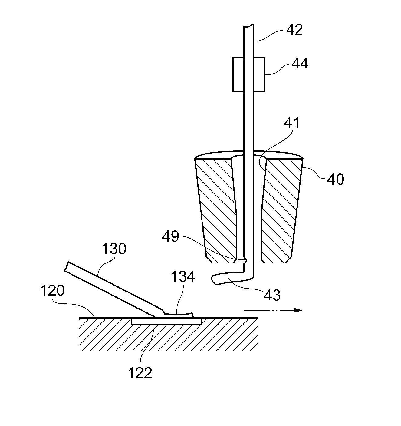
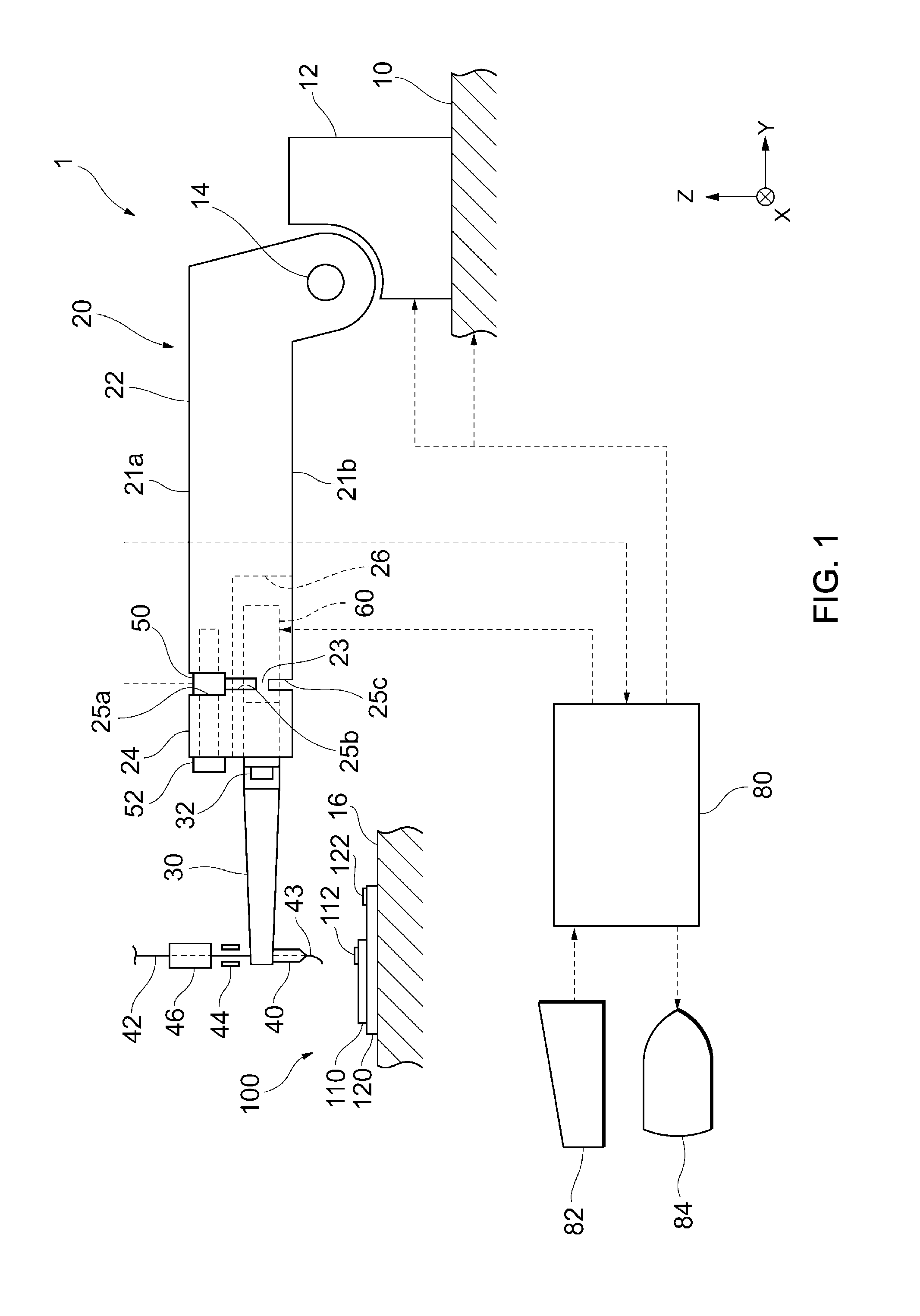
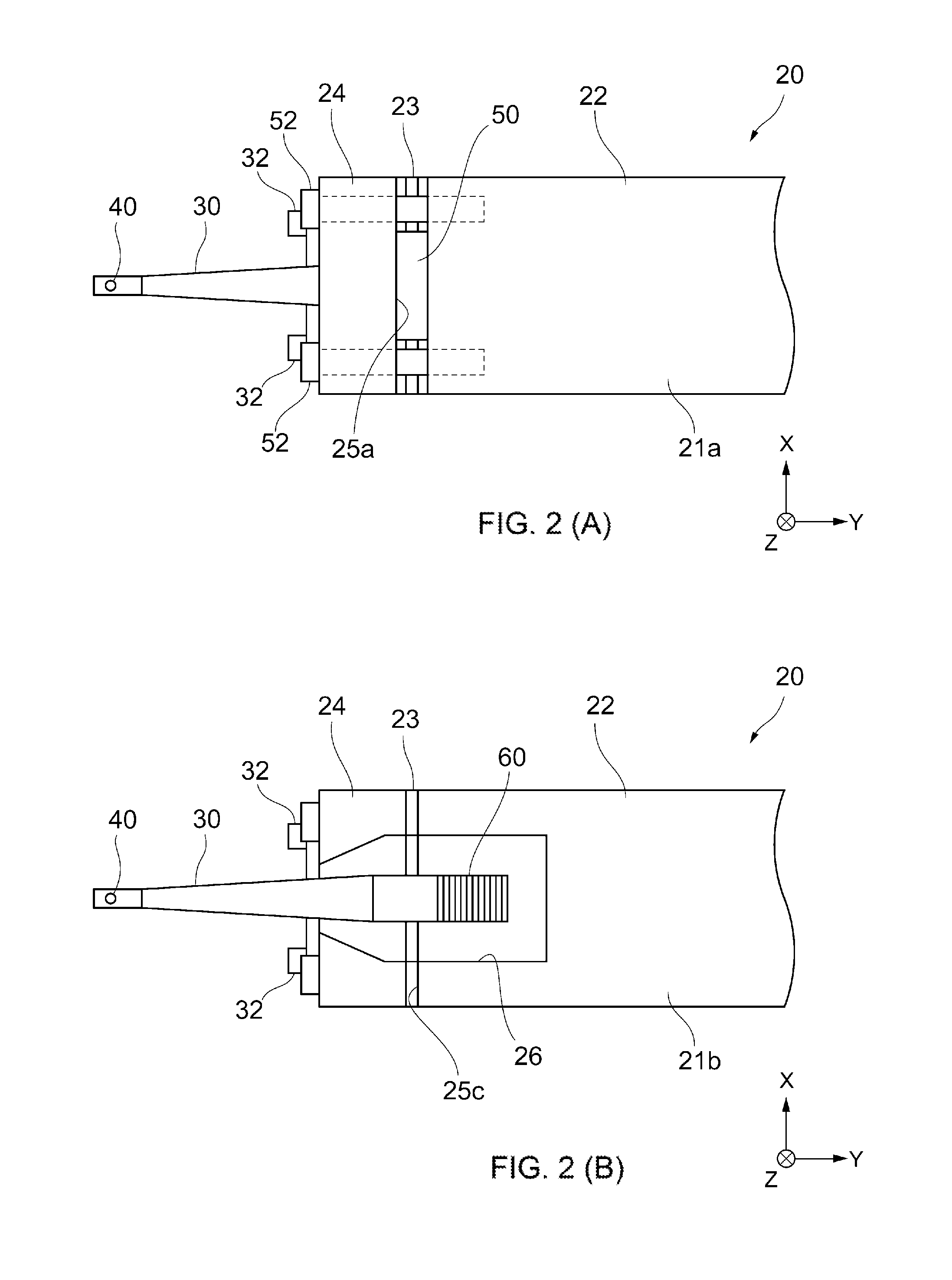
[0029]FIG. 1 illustrates a wire bonding apparatus according to an embodiment and FIG. 2 is a partially enlarged view of a bonding arm of the wire bonding apparatus, where FIG. 2 (A) is a top plan view of the bonding arm and FIG. 2 (B) is a bottom plan view of the bonding arm.

[0030]As shown in FIG. 1, the wire bonding apparatus 1 includes an XY drive mechanism 10, a bonding arm 20, an ultrasonic horn 30, a bonding tool 40, a load sensor 50, an ultrasonic vibrator 60, and a control unit 80.

[0031]The XY drive mechanism 10 is configured to be movable in the X and Y axis...


PUM


Abstract

A semiconductor device manufacturing method includes: raising and moving a bonding tool, while paying out a wire, in a direction from a second toward a first bonding point to form in the wire a cut portion bent in a vicinity of the second bonding point; lowering and moving a tip of the bonding tool to the cut portion; lowering the bonding tool vertically to thin the cut portion; raising the bonding tool while paying out the wire; and moving the bonding tool in a direction away from the first and second bonding points and along a wire direction connecting the first and second bonding points and then cutting the wire at the cut portion to form a wire tail. This allows the length of the wire tail to be adjusted easily and efficiently to be constant.

Description

CROSS REFERENCE TO RELATED APPLICATIONS[0001]This application is a Continuation of PCT International Application No. PCT / JP2015 / 053666, filed on Feb. 10, 2015, which claims priority under 35 U.S.C §119(a) to Patent Application No. 2014-032217, filed in Japan on Feb. 21, 2014, all of which are hereby expressly incorporated by reference into the present application.TECHNICAL FIELD[0002]The present invention relates to a semiconductor device manufacturing method, a semiconductor device, and a wire bonding apparatus.BACKGROUND ART[0003]In manufacturing of semiconductor devices, wire bonding is used commonly in which electrodes on a semiconductor chip and electrodes on a substrate, for example, are connected electrically using wires. As an aspect of such a wire bonding technique, there is known a wedge bonding system in which a wire is connected to a bonding target without forming a ball at the tip of the wire. In such a wedge bonding system, a first bonding point and a second bonding po...

Claims


Application Information

Patent Timeline
IPC IPC(8): H01L23/00
CPCH01L24/78H01L24/48H01L24/85H01L2224/78803H01L2224/85205H01L2224/7855H01L2224/48091H01L2224/48235H01L2224/48472H01L2224/78354H01L2224/73265H01L2224/78301H01L2924/15311H01L2924/00014H01L2224/05553H01L2224/78347H01L2224/78353H01L2224/7892H01L2224/78621H01L2224/02166H01L2224/85186H01L2224/32225H01L2224/48227H01L2224/48456H01L2224/78901H01L24/73H01L2224/45015H01L2924/207H01L2224/45099H01L2224/85399H01L2224/05599H01L2924/00012H01L21/76H01L24/03H01L24/04H01L2924/00
Inventor SEKINE, NAOKI
Owner SHINKAWA CO LTD
Why Eureka
Try Eureka