Solid-state imaging apparatus and charge transfer apparatus

Inactive Publication Date: 2005-08-11
RENESAS ELECTRONICS CORP
View PDF8 Cites 0 Cited by
  • Summary
  • Abstract
  • Description
  • Claims
  • Application Information

AI Technical Summary

Benefits of technology

[0024] According to one aspect of the present invention, there is provided a solid-state imaging apparatus which includes a photoelectric conversion section generating a charge by photoelectric conversion; and a charge transfer section having first and second transfer electrodes arranged in parallel with each other in an output direction of a charge generated by the photoelectric conversion section and repeatedly transferring the charge between a semiconductor region underneath the first transfer electrode and a semiconductor region underneath the second transfer electrode obliquely to an array direction of the first and second transfer electrodes to output the charge. Since this apparatus repeatedly transfers a charge between the first and second transfer electrodes arranged in parallel, the pitch of cells can be narrowed. Further, since a charge is transferred obliquely to the array direction of the first and second transfer electrodes, the entire charge transfer path is reduced to improve electron transfer efficiency.
[0025] According to another aspect of the present invention, there is provided a solid-state imaging apparatus which includes a plurality of photoelectric conversion sections generating a charge by photoelectric conversion; and a first transfer electrode array composed of a plurality of first transfer electrodes for transferring the charge, arranged in parallel with an array direction of the photoelectric conversion sections, and a second transfer electrode array composed of a plurality of second transfer electrodes for transferring the charge, arranged in parallel with the first transfer electrode array, wherein, in each of the first and the second transfer electrodes, two sides parallel to a direction perpendicular to the array direction of the photoelectric conversion sections have different lengths. Since this apparatus repeatedly transfers a charge between the first and second transfer electrodes arranged in parallel, the pitch of cells can be narrowed. Further, since a charge is transferred obliquely to the array direction of the first and second transfer electrodes, the entire charge transfer path is reduced to improve electron transfer efficiency.
[0026] According to still another aspect of the present invention, there is provided a solid-state imaging apparatus which includes a plurality of photoelectric conversion sections generating a charge by photoelectric conversion; and a plurality of first transfer electrodes arranged in parallel with an array direction of the photoelectric conversion sections, and a plurality of second transfer electrodes arranged in parallel with the array direction of the photoelectric conversion sections and adjacent to the first transfer electrodes, wherein the first and the second transfer electrodes are supplied with different drive signals for transferring the charge, and, when the first and the second transfer electrodes are supplied with the drive signals, a potential underneath the first and the second transfer electrodes is higher in an adjacent area of the first and the second transfer electrodes than in another area. Since this apparatus repeatedly transfers a charge between the first and second transfer electrodes arranged in parallel, the pitch of cells can be narrowed. Further, since a charge is transferred obliquely to the array direction of the first and second transfer electrodes, the entire charge transfer path is reduced to improve electron transfer efficiency.
[0027] The present invention provides a solid-state imaging apparatus and a charge transfer section with high electron transfer efficiency.

Problems solved by technology

Reduction of the unit cell size is thereby restricted by a design rule about electrode layout and a design rule about a connection of each electrode and a metal line such as the size of a contact, the inner margin of the end of a contact from the end of an electrode and so on, hindering the improvement of the resolution.
However, the CCD image sensor of FIG. 7 has the following problems.

Method used


Image

  • Solid-state imaging apparatus and charge transfer apparatus
  • Solid-state imaging apparatus and charge transfer apparatus
  • Solid-state imaging apparatus and charge transfer apparatus

Examples


first embodiment

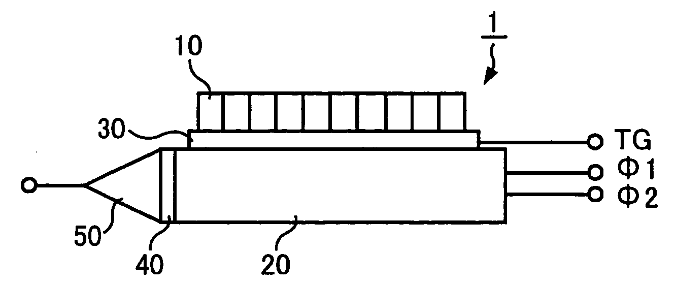
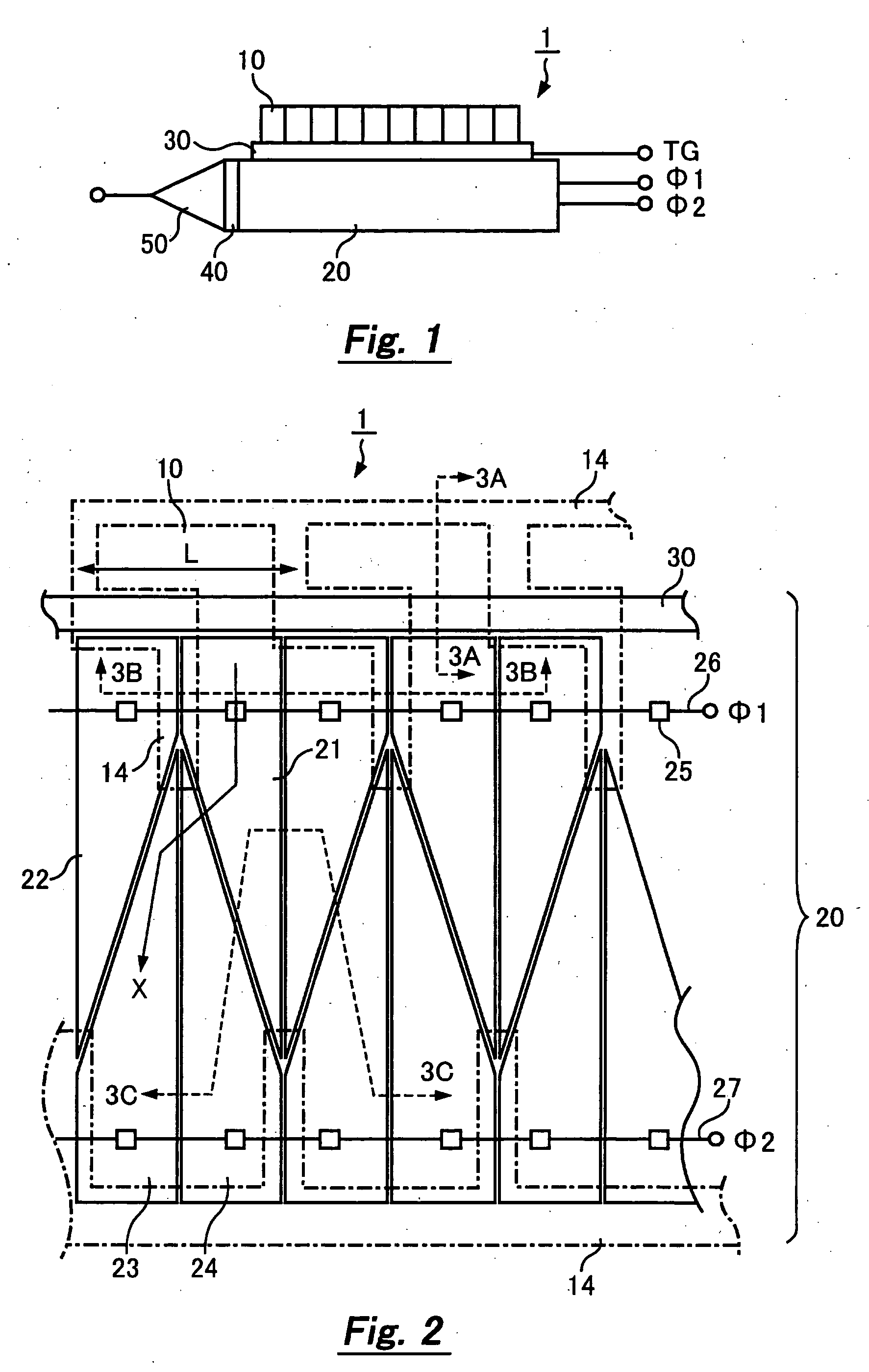
[0041] Referring first to FIGS. 1 to 3, the configuration of a CCD image sensor of the present invention is explained.

[0042]FIG. 1 is a schematic diagram of the CCD image sensor of this invention. The CCD image sensor 1 includes photodiodes 10, a transfer gate electrode 30, a CCD register 20, a charge detection section 40, and an output circuit 50. The photodiode 10 is a photoelectric conversion section that generates a charge by photoelectric conversion. The transfer gate electrode 30 is an electrode that passes the charge generated by the photodiodes 10 to the CCD register 20. The CCD register 20 is a charge transfer section or a charge transfer device that transfers the charge generated by the photodiode 10. The charge detection section 40 is a circuit that detects the charge transferred from the CCD register 20. The output circuit 50 is a circuit that outputs a signal according to the charge detected by the charge detection section 40 to the outside.

[0043] The CCD image sensor...

second embodiment

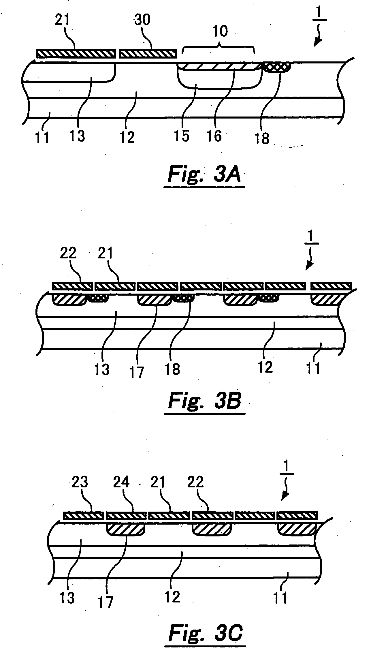
[0066] Referring now to FIG. 5, the configuration of the CCD image sensor according to a second embodiment of the invention is described. FIG. 5 is a plan view of the CCD image sensor of the second embodiment. Like FIG. 2, FIG. 5 is an enlarged view of the photodiodes 10, the transfer gate electrode 30, and the CCD register 20 of the CCD image sensor 1 shown in FIG. 1.

[0067] In FIG. 5, the same reference symbols as in FIG. 2 designate the same elements. Though the illustration of the contact 25 and the metal lines 26 and 27 are omitted in FIG. 5, the configuration is the same as in FIG. 2. The operation is the same as in FIGS. 4A and 4B if the electrodes 21 to 24 are replaced by electrodes 41 to 44.

[0068] The electrodes 41 to 44 have a rectangular shape as in the CCD image sensor of FIG. 7. The facing sides of the φ1 storage electrode 41 and the φ2 barrier electrode 44, and the facing sides of the φ1 barrier electrode 42 and the φ2 storage electrode 43 are parallel with the electr...


PUM


Abstract

A solid-state imaging apparatus includes a photoelectric conversion section generating a charge by photoelectric conversion; and a charge transfer section having first and second transfer electrodes arranged in parallel with each other in an output direction of a charge generated by the photoelectric conversion section and repeatedly transferring the charge between a semiconductor region underneath the first transfer electrode and a semiconductor region underneath the second transfer electrode obliquely to an array direction of the first and second transfer electrodes to output the charge.

Description

BACKGROUND OF THE INVENTION [0001] 1. Field of the Invention [0002] The present invention relates to solid-state imaging apparatus and particularly to a solid-state imaging apparatus having a charge transfer section which transfers charges generated by a photoelectric conversion section. [0003] 2. Description of Related Art [0004] A charge coupled device (CCD) image sensor formed on a semiconductor substrate and having a charge transfer function is widely used in faxes, scanners, copy machines, digital cameras and so on. The CCD image sensor sequentially outputs the signal charges accumulated according to the amount of light received by a photodetector such as a photodiode, thereby obtaining image information. [0005]FIG. 6 is a plan view of a conventional CCD image sensor. The CCD image sensor includes photodiodes 100, a transfer gate electrode 101, and a CCD register 102. A charge detection section and an output circuit, not shown, are placed in one end of the CCD register 102. [00...

Claims


Application Information

Patent Timeline
IPC IPC(8): H01L27/148H04N5/335H04N5/341H04N5/372
CPCH01L27/14806
Inventor MATSUYAMA, EIJI
Owner RENESAS ELECTRONICS CORP
Why Eureka
Try Eureka