

Stacked-type semiconductor device
- Summary
- Abstract
- Description
- Claims
- Application Information
AI Technical Summary
Benefits of technology
Problems solved by technology
Method used
Image

Examples
first embodiment
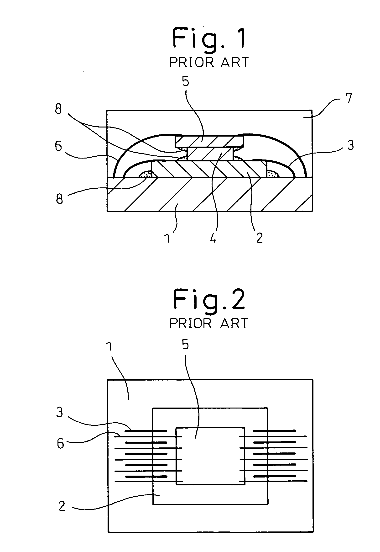
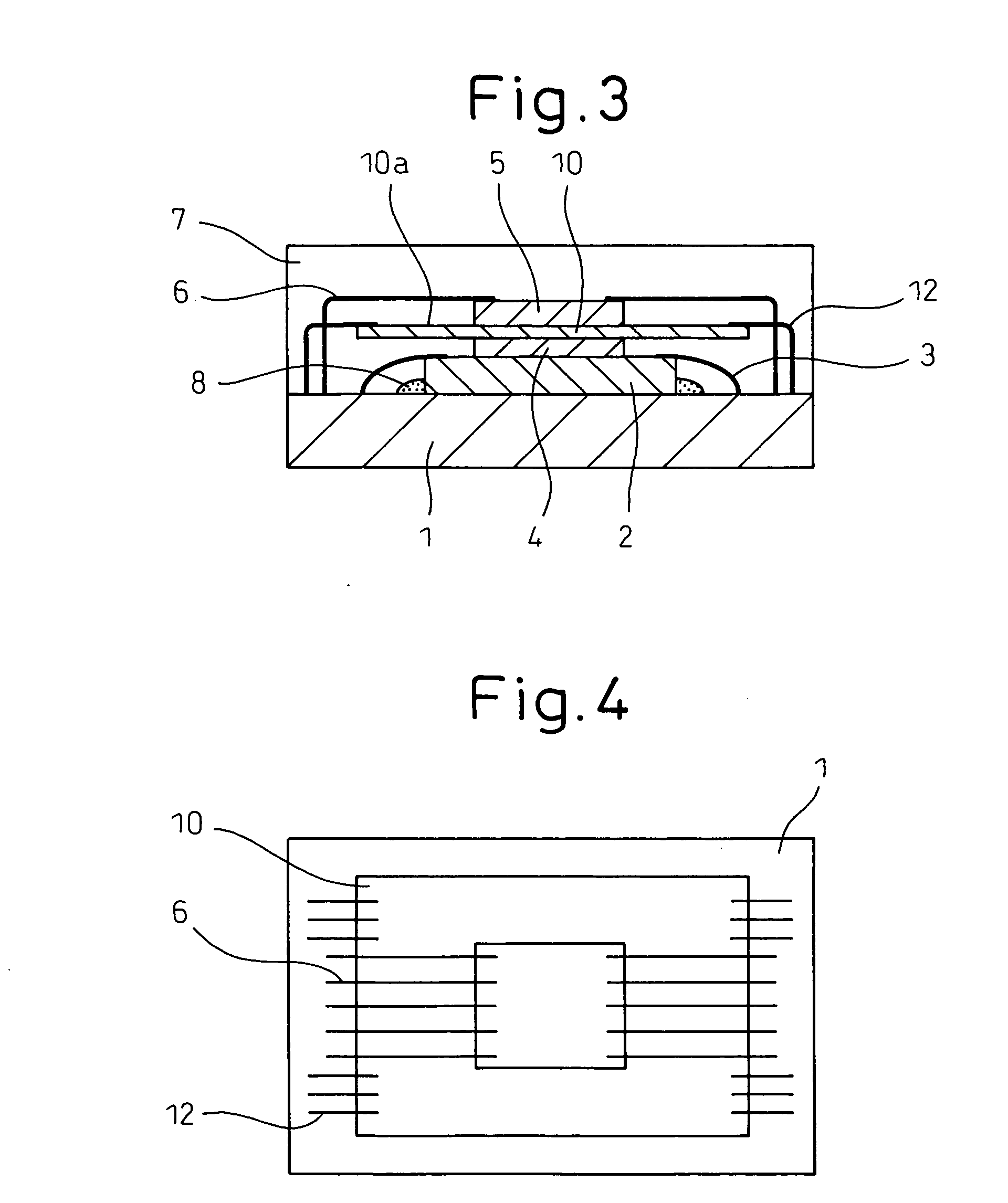
[0024]FIGS. 3 and 4 show a stacked-type semiconductor device according to the invention. A lower semiconductor element 2 is fixed on an element mounting area of the upper surface of a wiring board 1 using, for example, an adhesive 8, and the lower semiconductor element 2 and the wiring board 1 are electrically connected to each other by bonding wires 3 as required.
[0025] The signal electrode and the terminals of the lower semiconductor device 2 are arranged mainly in the surrounding area of the upper surface of the semiconductor element 2, and a spacer 4 of an insulating material such as ceramics is fixed in the central area of the upper surface of the semiconductor element 2 to secure a gap for the loop of the bonding wire 3, etc. The spacer 4 is a rectangular tabular member having an area smaller than the planar area of the lower semiconductor element 2 and has such a thickness that the parts mounted on the spacer 4 do not interfere with the loop of the bonding wire 3.
[0026] A ta...
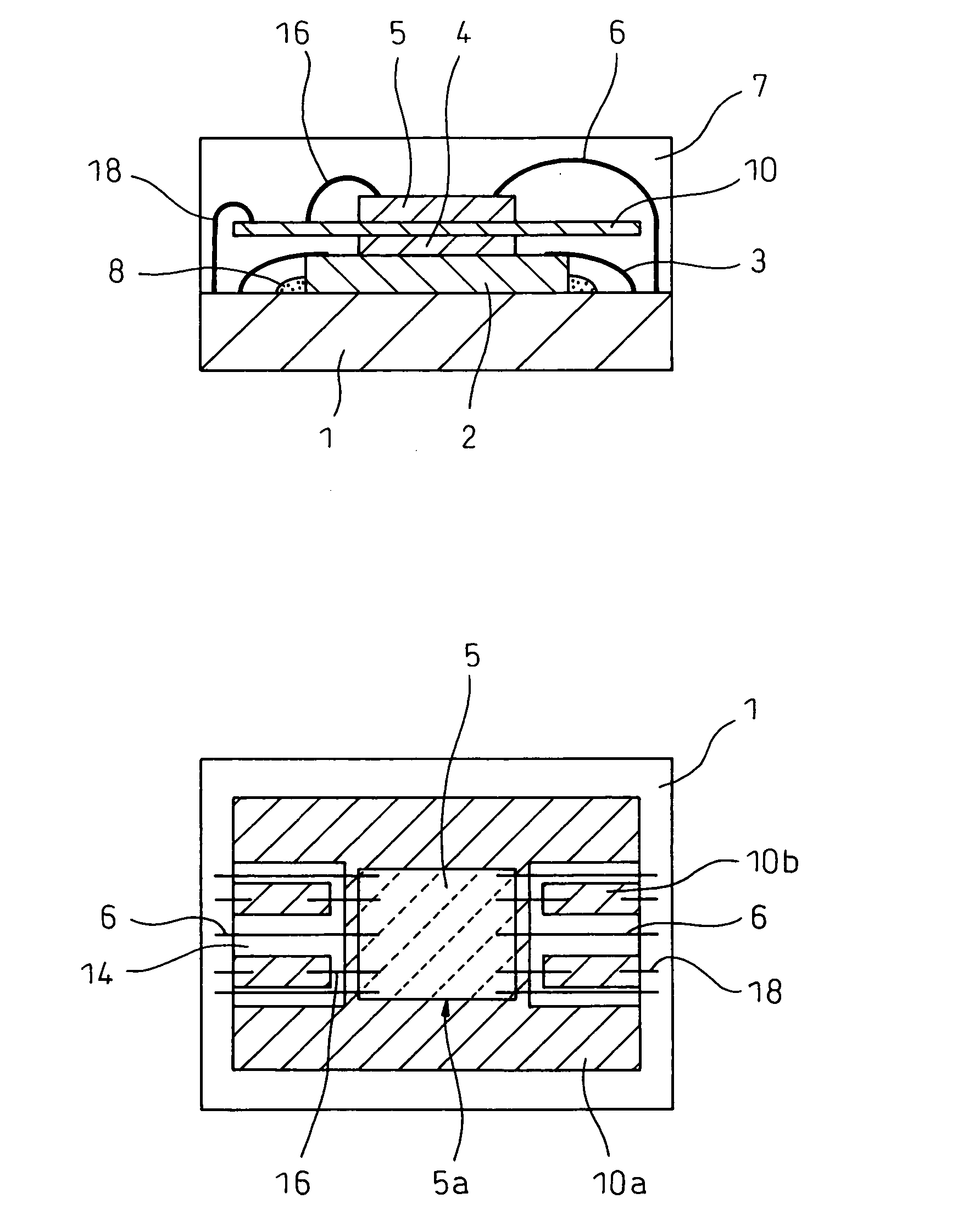
second embodiment
[0035] the signal conductor patterns 10b are formed, in addition to the grounding conductor film 10a, on the upper surface of the grounded spacer 10, and connected electrically to the signal electrode of the upper semiconductor element 5 through the conductor patterns 10b. In place of or in addition to the signal conductor patterns 10b, however, a power conductor pattern may be formed on the upper surface of the grounded spacer 10 and, through this conductor pattern, the electrical connection may be established with the power terminal of the upper semiconductor element 5.
[0036] The embodiments of the invention are explained above with reference to the accompanying drawings. This invention is not limited to these embodiments, however, and can be variously formed, modified or altered without departing from the spirit and scope thereof.
[0037] It will thus be understood from the foregoing description that according to this invention, there is provided a stacked-type semiconductor devi...
PUM
 Abstract
Description
Claims
Application Information