Production method for semiconductor device

a production method and semiconductor technology, applied in the direction of semiconductor devices, basic electric elements, electrical equipment, etc., can solve the problem of almost opaqueness and achieve the effect of accurate pattern

Inactive Publication Date: 2005-01-06
SONY CORP
View PDF2 Cites 16 Cited by
  • Summary
  • Abstract
  • Description
  • Claims
  • Application Information

AI Technical Summary

Benefits of technology

[0067] This method produces the following effect. The underlying layer remains flat when the etching mask having an opening pattern of the via holes is formed in step (e). The flat underlying layer permits the etching mask with an accurate pattern to be formed by ordinary lithography.

Problems solved by technology

Unfortunately, a metal film is almost opaque to light of ordinary wavelengths (200 to 1000 nm) used for mask alignment.

Method used


Image

  • Production method for semiconductor device
  • Production method for semiconductor device
  • Production method for semiconductor device

Examples


example 1

[0077] This example demonstrates the production method of a semiconductor device according to the first invention. FIGS. 1 to 2E are sectional views showing the sequential steps of forming the dual damascene structure according to the process in this example. For easy understanding, the same reference numerals are given to the parts in FIGS. 1 to 2E which correspond to the parts in FIGS. 5A to 5G. The same shall apply to FIGS. 3A to 4F.

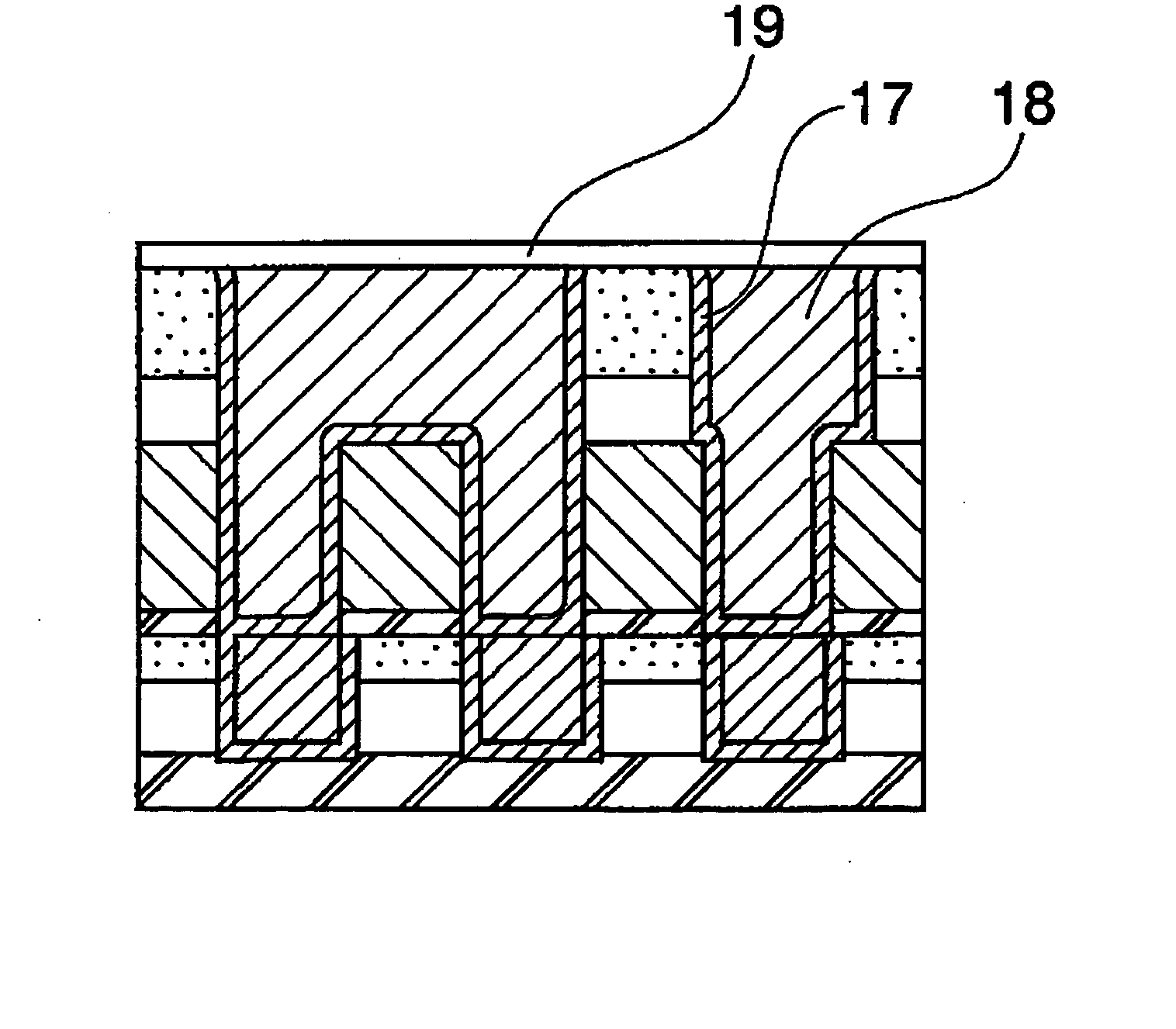
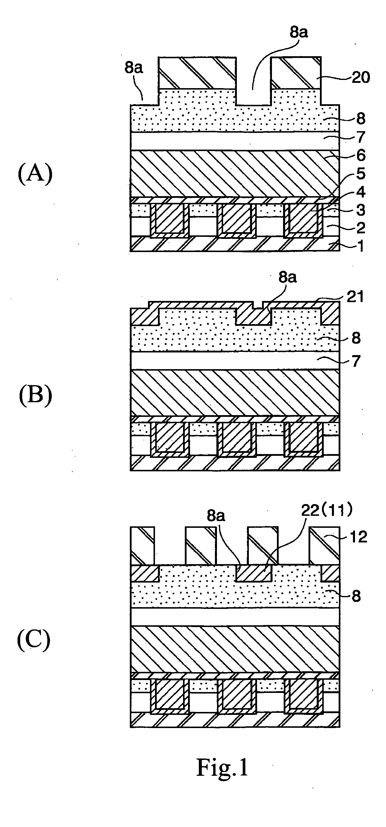
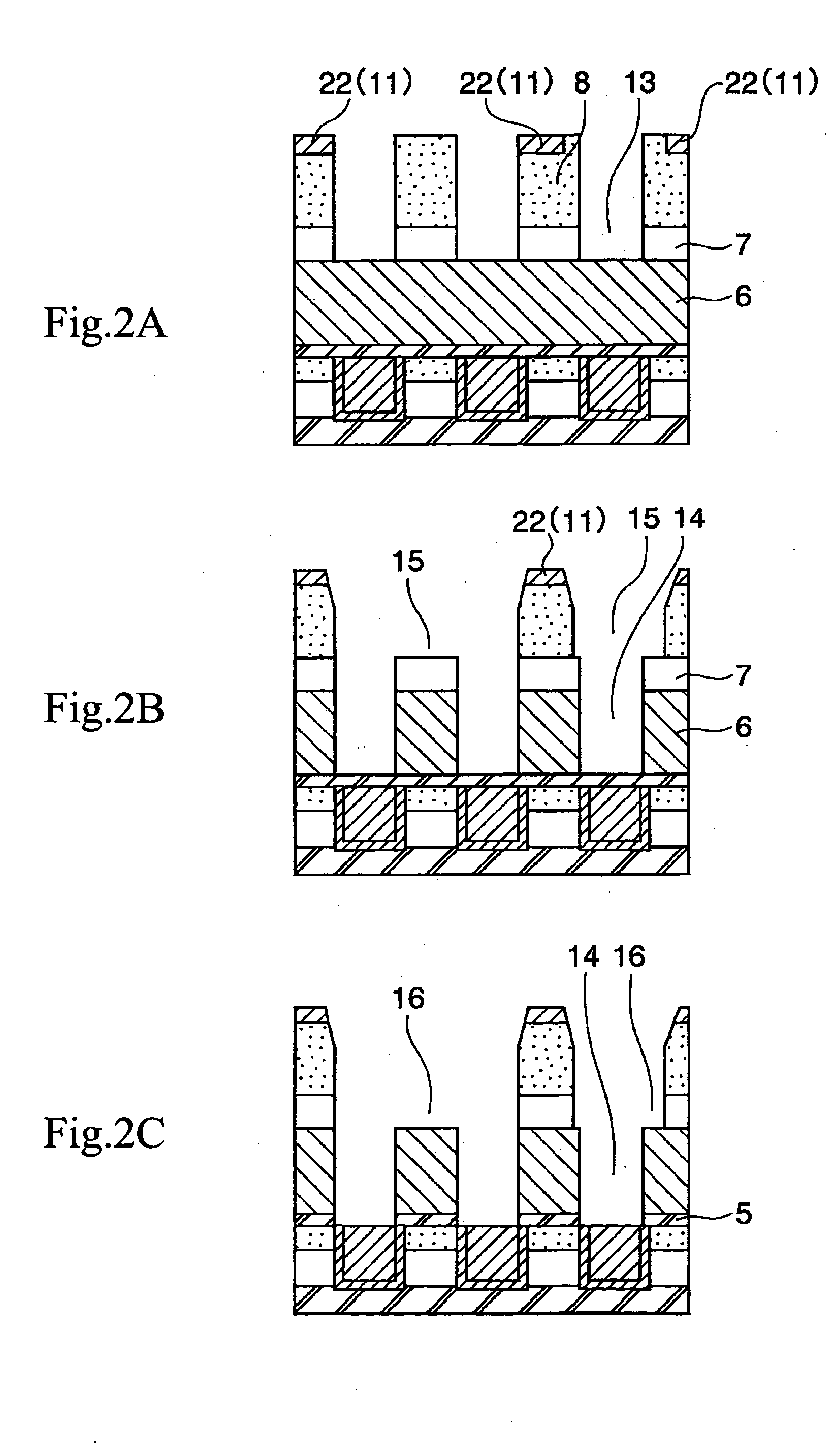
[0078] In the first step shown in (A) of FIG. 1, an underlying insulating film 1 is deposited on a substrate (not shown). On this underlying insulating film 1 is formed an interlayer insulating film which is a laminate film composed of an organic film 2 and a silicon oxide (SiO2) film 3. In this interlayer insulating film is formed a buried wiring 4 of copper (Cu) film which is 250 nm thick.

[0079] Then, on the Cu wiring 4 is formed an anti-oxidizing layer which is a 50-nm thick silicon carbide (SiC) film 5. On the anti-oxidizing layer is formed an i...

example 2

[0145] This example demonstrates the process for forming the dual damascene structure which is illustrated in section in FIGS. 3A to 3H.

[0146] As in example 1, the first step shown in FIG. 3A starts-with depositing an underlying insulating film 1 on a substrate (not shown). On this underlying insulating film 1 is formed an interlayer insulating film which is a laminate film composed of an organic film 2 and a silicon oxide (SiO2) film 3. In this interlayer insulating film is formed a buried wiring 4 of copper (Cu) film.

[0147] Then, on the Cu wiring 4 is formed an anti-oxidizing layer which is a 50-nm thick silicon carbide (SiC) film 5. On the anti-oxidizing layer are formed a carbon-containing silicon oxide (SiOC) film 6 (400 nm thick) and a polyaryl ether (PAE) film 7 (200 nm thick) as an organic polymer layer having a dielectric constant of about 2.6.

[0148] Further, on the PAE film 7 is formed a first mask forming layer 8 which is a 150-nm thick SiO2 film.

[0149] In this exampl...

example 3

[0187] This example demonstrates the process for forming the dual damascene structure which is illustrated in section in FIGS. 4A to 4F.

[0188] As in example 1, the first step shown in FIG. 4A starts with depositing an underlying insulating film 1 on a substrate (not shown). On this underlying insulating film 1 is formed an interlayer insulating film which is a laminate film composed of an organic film 2 and a silicon oxide (SiO2) film 3. In this interlayer insulating film is formed a buried wiring 4 of copper (Cu) film.

[0189] Then, on the Cu wiring 4 is formed an anti-oxidizing layer which is a 50-nm thick silicon carbide (SiC) film 5. On the anti-oxidizing layer are formed a carbon-containing silicon oxide (SiOC) film 6 (400 nm thick) and a polyaryl ether (PAE) film 7 (200 nm thick) as an organic polymer layer having a dielectric constant of about 2.6.

[0190] Further, on the PAE film 7 is formed a first mask forming layer 8 which is a 150-nm thick SiO2 film.

[0191] In this exampl...


PUM


Abstract

Disclosed herein is a production method of a semiconductor device having multilayer interconnections of well-formed dual damascene structure in the low dielectric constant interlayer insulating film.
The method includes a step of forming on an underlayer wiring a first insulating film, a second insulating, and first mask forming layer; a step of forming a first resist mask (20) having an inverted pattern of wiring trenches for the upper wiring; a step of etching the first mask forming layer through the first resist mask, thereby forming in the first mask forming layer a concave part conforming to the inverted pattern of wiring trenches for the upper wiring, and then forming on the first mask forming layer a second mask forming layer, thereby filling the concave part with the second mask forming layer; a step of selectively removing the second mask forming layer on the region in which the wiring trench is formed, thereby forming the second mask having the wiring trench pattern; a step of forming on the first mask forming layer a second resist mask (12) having an opening pattern of the via holes; a step of etching the first mask forming layer and the second insulating film through the second resist mask, thereby forming the via holes. This process is followed by the ordinary procedure to form the dual damascene structure.

Description

TECHNICAL FIELD [0001] The present invention relates to a production method of a semiconductor device having multilayer interconnections of dual damascene structure in the low dielectric constant interlayer insulating film, and more particularly, to a production method of a semiconductor device having interconnections of dual damascene structure in proper form. BACKGROUND ART [0002] The ever increasing degree of size reduction and integration in semiconductor devices has posed a serious problem with delay in electric signals resulting from the time constant of interconnections. A solution to this problem is the replacement of aluminum (Al) alloy by copper (Cu) having a lower electric resistance for conductive layers in multilayer interconnection. [0003] Unlike Al, which is a conventional metallic material used for multilayer interconnections, Cu presents difficulties in patterning by dry etching. Consequently, Cu multilayer interconnections are usually obtained by the damascene tech...

Claims


Application Information

Patent Timeline
Patent Type & Authority Applications(United States)
IPC IPC(8): H01L21/4763H01L21/768
CPCH01L21/76811H01L21/76813Y10S438/942H01L21/76829H01L21/76835H01L21/76825
Inventor KANAMURA, RYUICHI
Owner SONY CORP
Why Eureka
Try Eureka