

Semiconductor process
a technology of semiconductors and process steps, applied in the direction of semiconductor devices, basic electric elements, electrical equipment, etc., can solve the problems of serious leakage current and current decrease, and achieve the effect of accurate pattern transfer and reduced pattern line width
- Summary
- Abstract
- Description
- Claims
- Application Information
AI Technical Summary
Benefits of technology
Problems solved by technology
Method used
Image

Examples
first embodiment
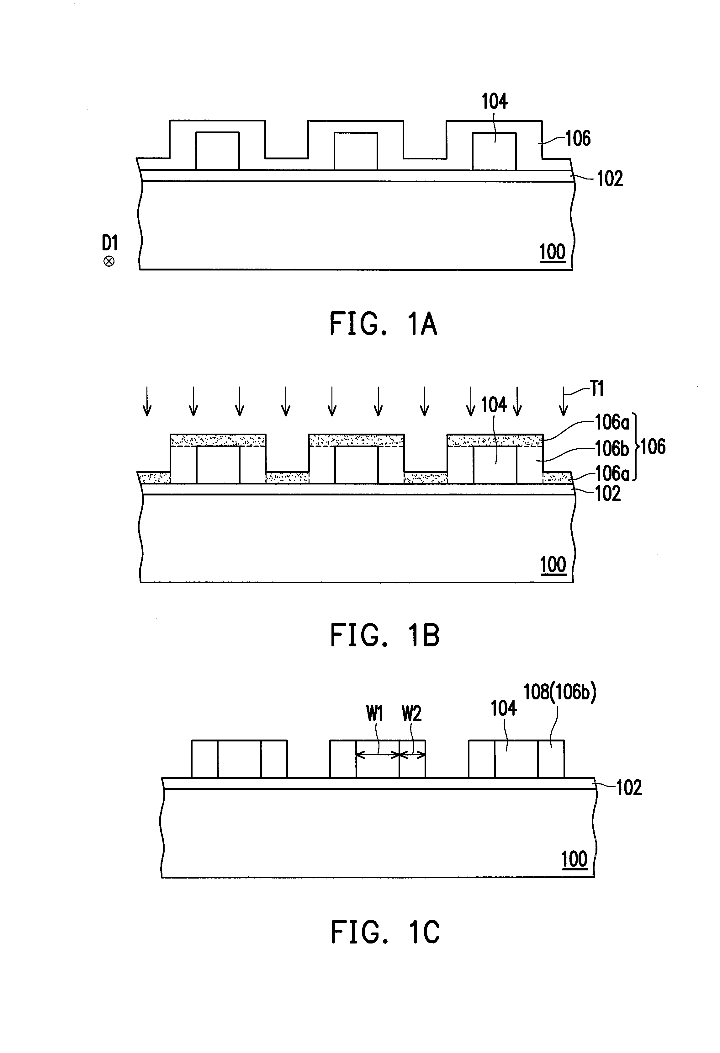
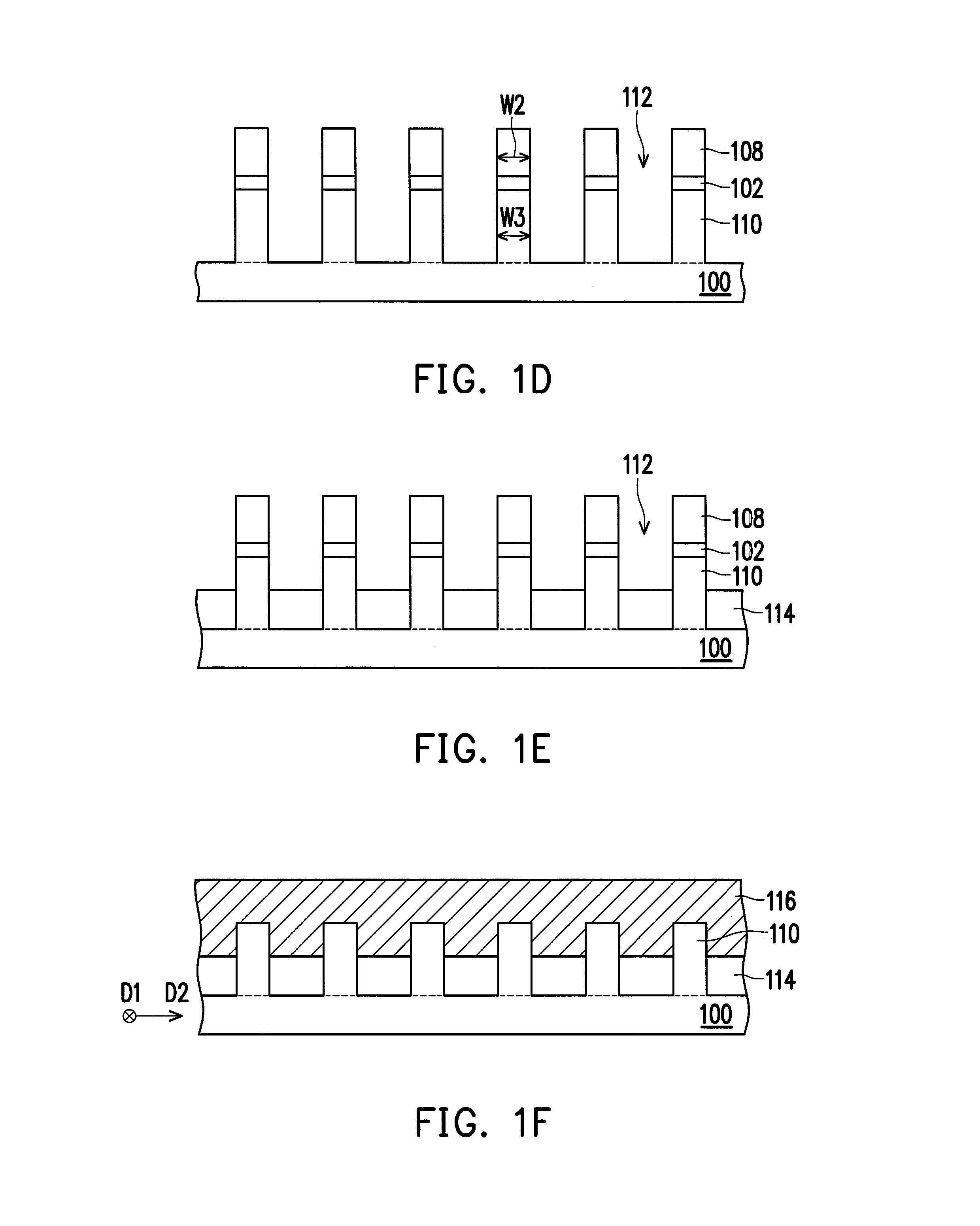
[0033]FIGS. 1A to 1F schematically illustrate cross-sectional views of a semiconductor process according to a first embodiment of the present invention. FIG. 1G schematically illustrates a top view of the structure layout of FIG. 1F, wherein only main components of fin structures, a gate, sources and drains are shown to simply the figure.
[0034]Referring to FIG. 1A, a substrate 100 such as a bulk wafer is provided. It is noted that in FIG. 1A, a bulk wafer is provided for illustration purposes, but the present invention is not limited thereto. In another embodiment, the substrate 100 can be a silicon on insulator (SOI) wafer. The material of the substrate 100 is selected from the group consisting of silicon (Si), germanium-doped silicon (Ge-doped Si), carbon-doped silicon (C-doped Si), SiGe, germanium (Ge), and III-V semiconductor such as GaAs, InGaAs, InSb, InAs, GaSb, InP, etc. Thereafter, a pad layer 102 is optionally formed on the substrate 100, so as to improve adhesion of dummy...
second embodiment
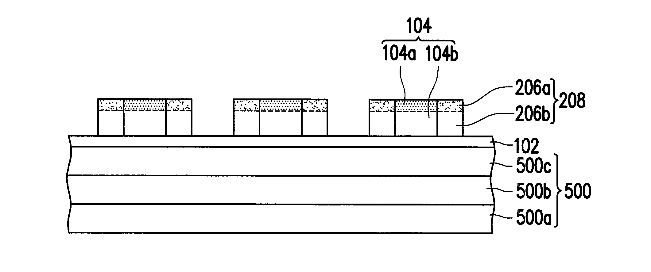
[0045]FIGS. 2A to 2D schematically illustrate cross-sectional views of a semiconductor process according to a second embodiment of the present invention. FIG. 2A describes the step after FIG. 1A of the first embodiment. The same reference numbers denote the same components and the details are not iterated herein.
[0046]Referring to FIG. 2A, after the mask material layer 106 is conformally formed on the substrate 100, recesses 202 are formed in the mask material layer 106 between adjacent dummy patterns 104. Thereafter, a photoresist layer 204 is formed on the mask material layer 106 between two adjacent dummy patterns 104, so as to at least expose the mask material layer 106 on the dummy patterns 104. Specifically, the photoresist layer 204 fills in the recesses 202 of the mask material layer 106, and the top surface of the photoresist layer 204 is substantially as high as the top surfaces of the dummy patterns 104, so as to expose the surface of the mask material layer 106 substanti...
third embodiment
[0053]FIGS. 3A to 3D schematically illustrate cross-sectional views of a semiconductor process according to a third embodiment of the present invention. The process steps and sequence in FIGS. 3A to 3D are similar to those in FIGS. 2A to 2D. The same reference numbers denote the same components and the details are not iterated herein.
[0054]Referring to FIG. 3A, the main difference between the second and third embodiments lies in that before the step of forming the mask material layer 106, a plurality of hard mask layers 302, in this embodiment, are respectively formed on the dummy patterns 104. Therefore, the subsequently formed mask material layer 106 can cover the hard mask layers 302, the pad layer 102 and the substrate 100. The material of the hard mask layers 302 is silicon nitride or silicon oxide, for example. The method of forming the dummy patterns 104 and the hard mask layers 302 includes sequentially depositing material layers for forming the dummy patterns 104 and the ha...
PUM
 Abstract
Description
Claims
Application Information