

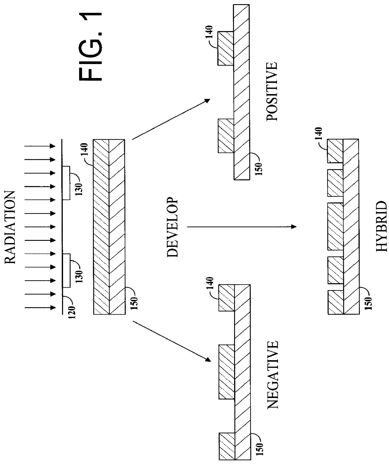
Method for forming transistors with raised source and drains and device formed thereby
a transistor and source technology, applied in the field of transistors with raised sources and drains, can solve the problems of junction capacitance and low leakage, and achieve the effect of increasing the performance of the transistor and facilitating the formation of field effect transistors
- Summary
- Abstract
- Description
- Claims
- Application Information
AI Technical Summary
Benefits of technology
Problems solved by technology
Method used
Image

Examples
example 2
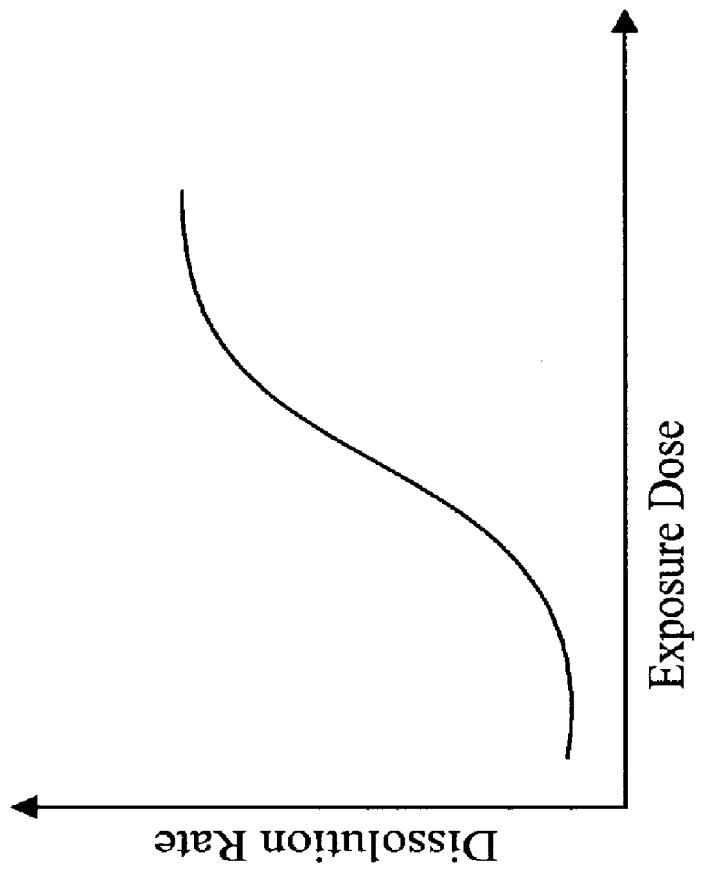
This example illustrates the manner in which changing the type of photoacid generator and relative amounts of the various components can change the dissolution rate characteristics of the hybrid resist and subsequently the lithographic response. This second formulation was prepared and processed in a manner similar to EXAMPLE 1, however, it is comprised of the following components:
PHS with about 25% of the phenol groups protected with MOP, 90.8% of solids;
triphenyl sulfonium triflate, 1.3% of solids;
Powderlink, 7.8% of solids;
tetrabutyl ammonium hydroxide base, 0.1% of solids; and
sufficient PM acetate containing 350 ppm FC-430 surfactant as a solvent to form a 18.9% solids solution.
The dissolution rate characteristic of the resulting hybrid resist is shown in FIG. 14. The overall nature of the curve remains similar to that shown by the hybrid resist of EXAMPLE 1, in that the dissolution rate starts out low for an unexposed resist, increases to a high at about 5 mJ and decreases to a...
example 3
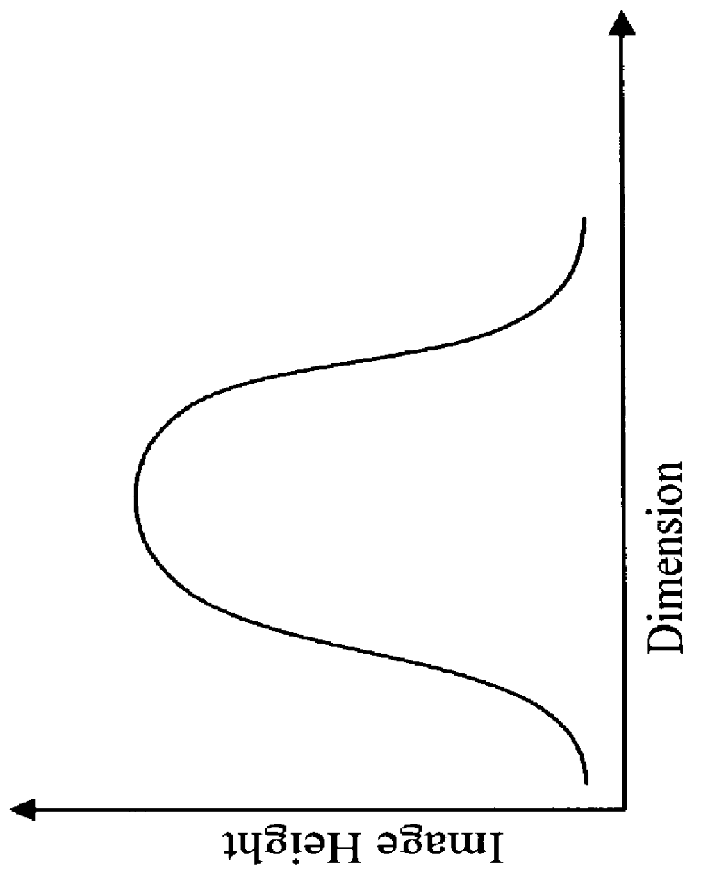
This example illustrates that the space width of the frequency doubled image can be changed by varying the protection level of PHS with MOP. Two different PHS lots having 24% and 15% MOP loading, respectively, were used to make hybrid formulations identical to that of EXAMPLE 1, except that the total solids contents were adjusted to 16.0% of the total to obtain film thicknesses of about 0.5 .mu.m. From these two stock formulations, several other formulations with average MOP levels ranging from 15 to 24% were prepared. Wafers were coated and soft baked at 110.degree. C., exposed on a MICRASCAN II DUV 0.5 NA stepper, post exposed baked at 110.degree. C. for 60 sec and finally developed with 0.14N TMAH developer. A reticle with an isolated chrome opening was printed in a hybrid resist film. The spacewidth of the resist image was measured and graphed as a function of the average MOP solubility inhibitor loading in the PHS used for making the respective formulations. It was found that t...
example 4
Negative tone imaging may be performed with the hybrid resist of the present invention, using a blanket DUV expose after the PEB and prior to the develop.
A hybrid resist formulation as described in EXAMPLE 2, above, was image-wise exposed with a chrome reticle with an electrical test pattern on a 0.5NA DUV expose system. Silicon wafers (200 mm) with a 2000 Angstrom (.ANG.) film of polysilicon were used as a substrate so that the resulting etched patterns of the resist image could be measured with electrical probe techniques. After the post expose bake process, the wafers were cycled back into the expose tool (MICRASCAN II) and exposed at 10 mJ per square centimeter (cm.sup.2)with a clear glass reticle. A post expose bake process was not performed after the second exposure. The purpose of the second exposure was to remove the initially unexposed resist from the wafer, leaving only a negative tone resist pattern after develop.
The initial image-wise expose dose was 17-24 mJ / cm2, the po...
PUM
| Property | Measurement | Unit |
|---|---|---|
| thickness | aaaaa | aaaaa |
| size | aaaaa | aaaaa |
| molecular weight | aaaaa | aaaaa |
Abstract
Description
Claims
Application Information