Method of treating inlaid copper for improved capping layer adhesion without damaging porous low-k materials

a technology of inlaid copper and low-k materials, which is applied in the direction of basic electric elements, semiconductor/solid-state device manufacturing, electric devices, etc., can solve the problems of reducing affecting the adhesion of the capping layer, and exhibiting poor adhesion to the cu or cu alloy surface, so as to reduce the parasitic rc time delay

Inactive Publication Date: 2005-04-05
GLOBALFOUNDRIES INC
View PDF5 Cites 23 Cited by
  • Summary
  • Abstract
  • Description
  • Claims
  • Application Information

AI Technical Summary

Benefits of technology

An advantage of the present invention is a method of fabricating a semiconductor device having interconnect patterns exhibiting reduced parasitic R×C time delays employing porous dielectric materials having a low dielectric constant.
Another advantage of the present invention is a method of fabricating a semiconductor device comprising reliably capped Cu or Cu alloy interconnects in porous low-k dielectric layers without degradation or etching of the low-k dielectric layers.
Additional advantages and other features of the present invention will be set forth in the description which follows and in part will be apparent to those having ordinary skill in the art upon examination of the following or may be learned from the practice of the present invention. The advantages of the present invention may be realized and obtained as particularly pointed out in the appended clams.
According to the present invention, the foregoing and other advantages are achieved in part by a method of fabricating a semiconductor device, the method comprising: forming an opening in an upper surface of a porous low-k dielectric layer; filling the opening with copper (Cu) or a Cu alloy; conducting chemical-mechanical polishing (CMP) leaving the upper surface of the Cu or Cu alloy exposed; and treating the upper surface of the Cu or Cu alloy with a plasma while controlling plasma conditions to avoid etching the upper surface of the porous low-k material.
Embodiments of the present invention include forming a dual damascene opening in a dielectric layer having a dielectric constant (k) no greater than 2.4, and typically having a k value of 2.0 to 2.2, depositing a barrier metal layer, such as tantalum, tantalum nitride or a composite layer of tantalum nitride and alpha (α)-tantalum, filling the opening with Cu or Cu alloy, with or without the use of a seedlayer, conducting CMP leaving an upper surface of the Cu or Cu alloy exposed and containing a layer of copper oxide thereon, and treating the upper surface with an NH3 or H2 plasma at a power of 75 to 125 watts for 2 to 8 seconds to remove the layer of copper oxide while preventing etching and / or degradation of the porous low-k material. Subsequently, a capping layer, such as silicon nitride or silicon carbide, is deposited, typically at a thickness of 250 Å to 550 Å.

Problems solved by technology

Interconnection technology is constantly challenged to satisfy the ever increasing requirements for high density and performance associated with ultra large scale integration semiconductor devices.
Additional problems have been encountered attendant upon conventional Cu interconnect methodology employing a diffusion barrier layer (capping layer).
For example, it was found that after conducting chemical-mechanical polishing (CMP) of an inlaid Cu or Cu alloy layer, a deposited capping layer, such as silicon nitride, exhibited poor adhesion to the Cu or Cu alloy surface.
Such poor adhesion rendered the capping layer vulnerable to removal, as by peeling due to scratching or stresses resulting from subsequent processing.
Consequently, the Cu or Cu alloy is not entirely encapsulated resulting in Cu diffusion, thereby adversely impacting device performance and decreasing the electromigration resistance of the interconnect.
However, upon conducting experimentation into the use of copper interconnect technology using porous low-k materials, it was found that such NH3 and H2 plasma treatment degraded the porous low-k material.
The upper surface of the inlaid copper has an undesirable layer of a copper oxide 15, which adversely impacts capping layer adhesion.
3 and an undesirable step “D” of up to 2,000 Å. Such irregular surface typography generates various problems, such as an undesirable significant reduction in the thickness of the ILD, degradation of the low-k property of the ILD and extremely poor within-wafer thickness uniformity.

Method used


Image

  • Method of treating inlaid copper for improved capping layer adhesion without damaging porous low-k materials
  • Method of treating inlaid copper for improved capping layer adhesion without damaging porous low-k materials
  • Method of treating inlaid copper for improved capping layer adhesion without damaging porous low-k materials

Examples


Embodiment Construction

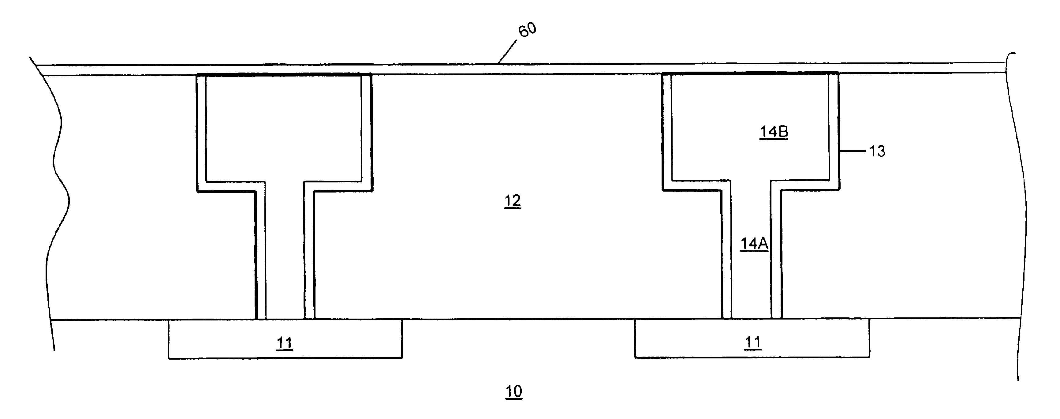
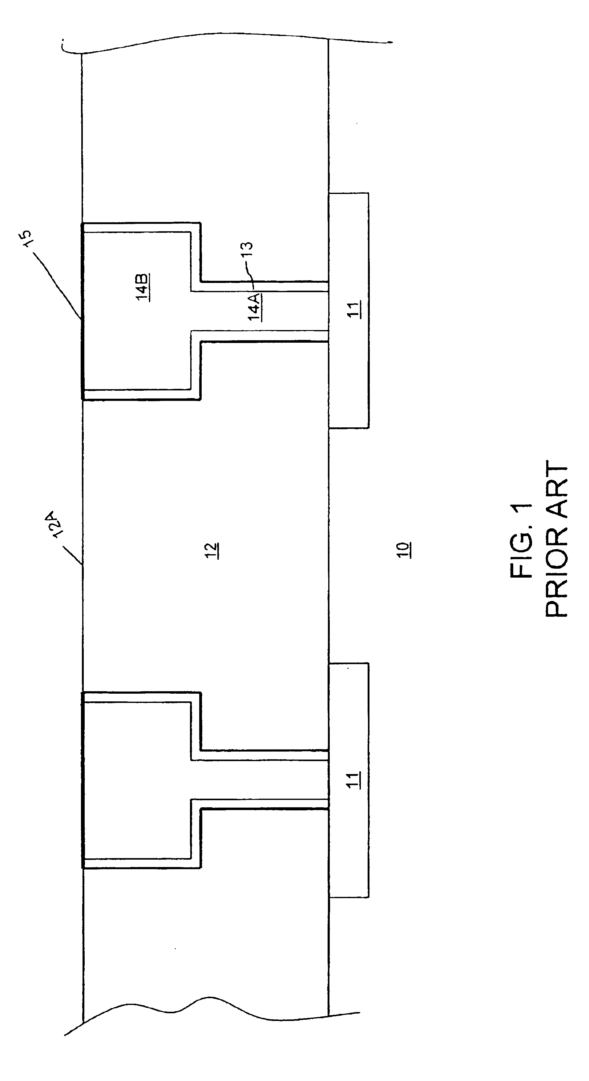
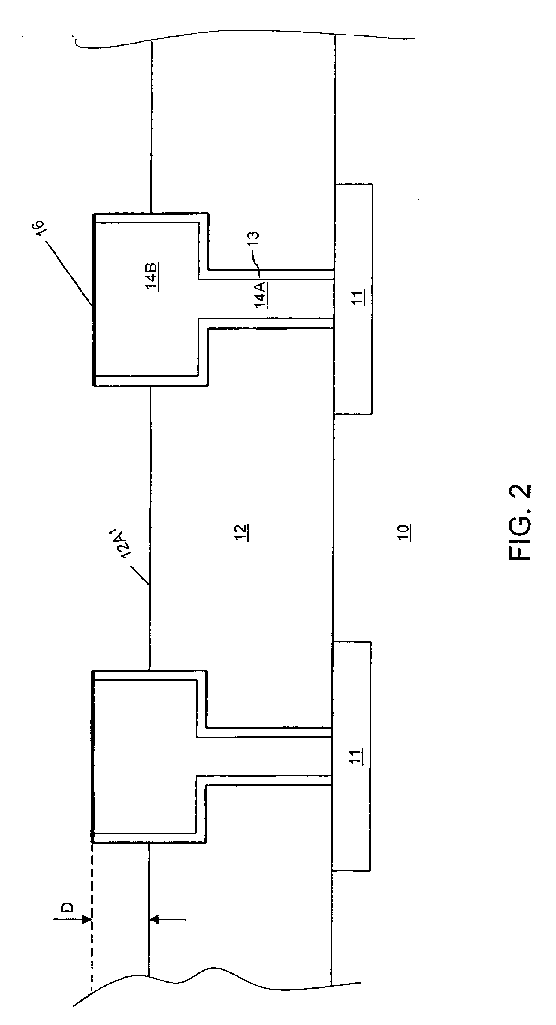
The present invention addresses and solves problems attendant upon fabricating multi-layer interconnect devices, particularly parasitic R×C time delays. The capacitance, both layer-to-layer and within-layer, is primarily attributed to the film properties of the ILD. The present invention enables efficient implementation of multi-level interconnect technology using Cu and / or Cu alloys with various porous low-k dielectric materials for ILDs, by providing methodology enabling formation of reliably capped Cu and / or Cu alloy interconnects, without or with significantly reduced degradation and / or etching of the porous low-k dielectric materials. As employed throughout this disclosure, the symbol Cu is intended to encompass high purity elemental copper as well as copper-based alloys, such as copper alloys containing minor amounts of tantalum indium, tin, zinc, manganese, titanium, germanium, zirconium, strontium, palladium, magnesium, chromium and tantalum.

Experimentation and investigation...


PUM

PropertyMeasurementUnit
poweraaaaaaaaaa
dielectric constantaaaaaaaaaa

Abstract

An exposed surface of inlaid Cu is plasma treated for improved capping layer adhesion while controlling plasma conditions to avoid damaging porous low-k materials. Embodiments include forming a dual damascene opening in a porous dielectric material having a dielectric constant (k) of up to 2.4, e.g., 2.0 to 2.2, filling the opening with Cu, conducting CMP, plasma treating the exposed Cu surface in NH3 or H2 at a low power, e.g., 75 to 125 watts, for a short period of time, e.g., 2 to 8 seconds, without etching the porous low-k material and depositing a capping layer, e.g., silicon nitride or silicon carbide.

Description

FIELD OF THE INVENTIONThe present invention relates to a method of treating copper (Cu) and / or Cu alloy metallization for improved capping layer adhesion without damaging associated porous low-k materials. The present invention is particularly applicable in fabricating high-speed integrated circuits having sub-micron designed features and reliable high conductivity interconnect structures.Interconnection technology is constantly challenged to satisfy the ever increasing requirements for high density and performance associated with ultra large scale integration semiconductor devices. The speed of semiconductor circuitry varies inversely with the resistance (R) and capacitance (C) of the interconnection system. The higher the value of the R×C product, the more limiting the circuit speed. As integrated circuits become more complex and feature sizes and spacings become smaller, the integrated circuit speed becomes less dependent upon the transistor itself and more dependent upon the int...

Claims


Application Information

Patent Timeline
Patent Type & Authority Patents(United States)
IPC IPC(8): H01L21/44H01L21/02H01L21/768
CPCH01L21/76877H01L21/76834H01L21/76807
Inventor NGO, MINH VANHUERTAS, ROBERTPHAM, HIEU
Owner GLOBALFOUNDRIES INC
Why Eureka
Try Eureka