

Organic el device, method of manufacturing organic el device, and electronic apparatus
a technology of organic el and el, which is applied in the manufacture of electric discharge tubes/lamps, discharge tubes luminescnet screens, instruments, etc., can solve the problems of deteriorating symmetry on viewing angle characteristics, low actual use efficiency of photosensitive resin materials, and remarkable problems, etc., to achieve excellent display quality
- Summary
- Abstract
- Description
- Claims
- Application Information
AI Technical Summary
Benefits of technology
Problems solved by technology
Method used
Image

Examples
first embodiment
Organic EL device
[0053]First of all, an organic EL device of the present embodiment will be described with reference to FIGS. 1 to 4.
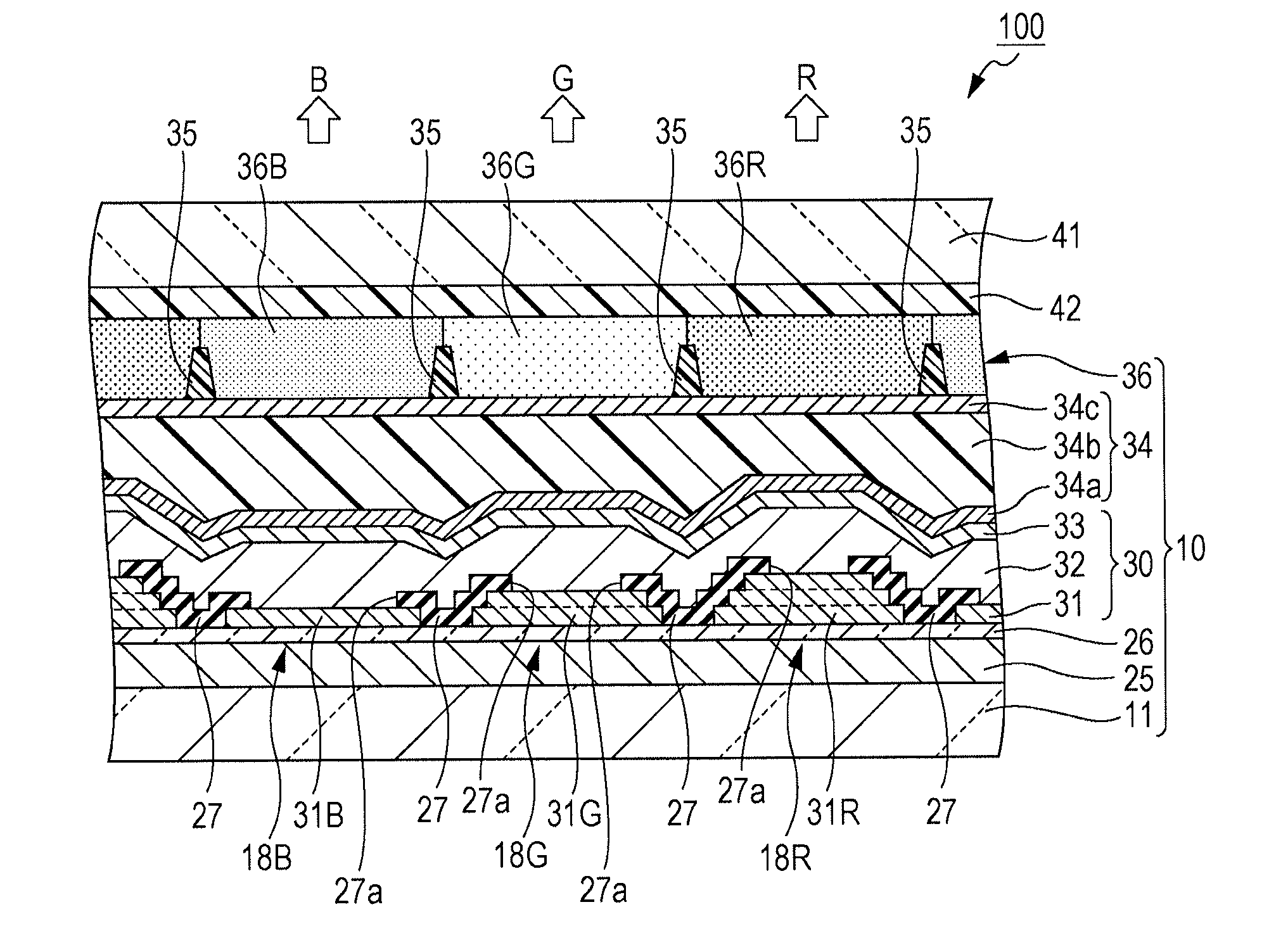
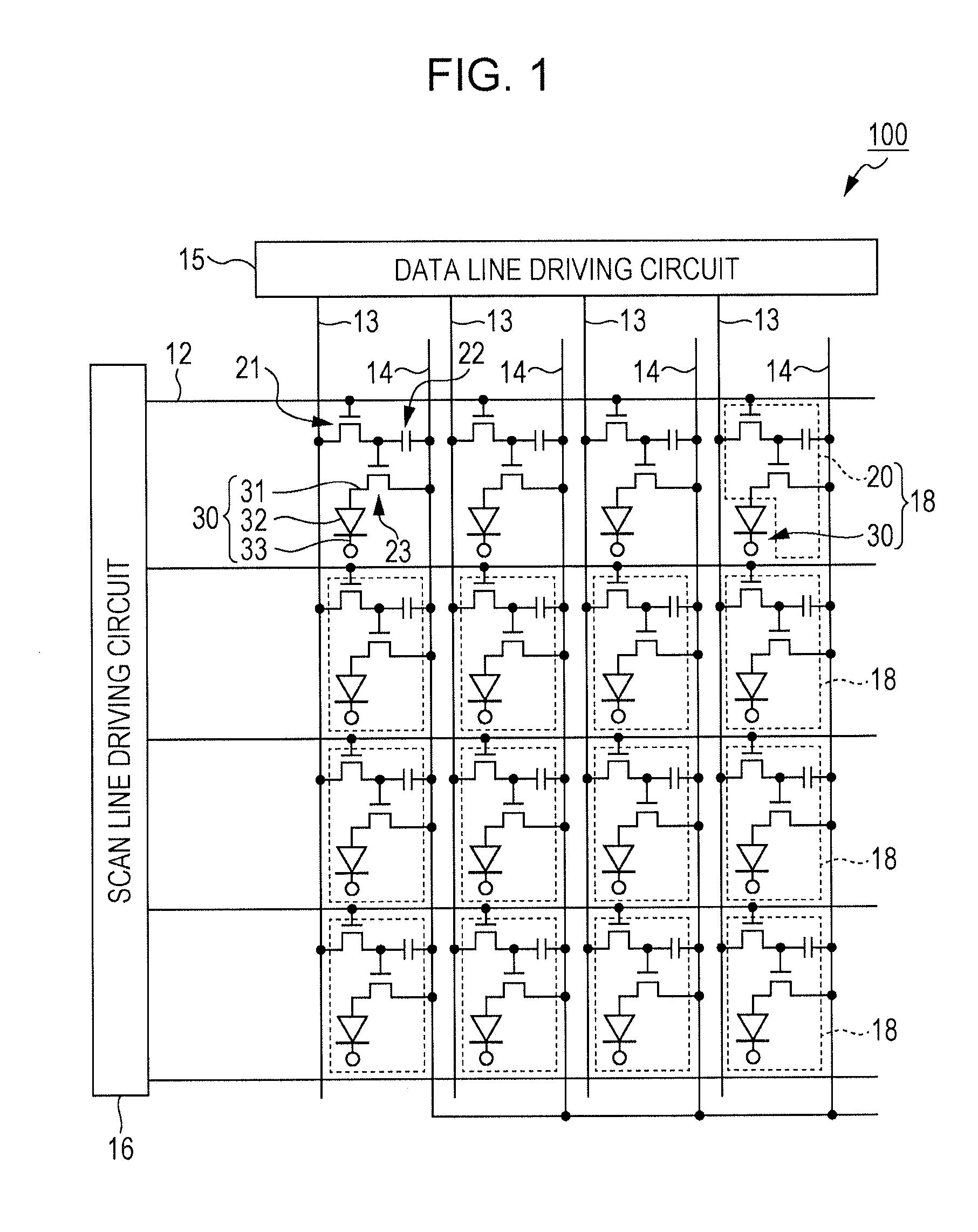
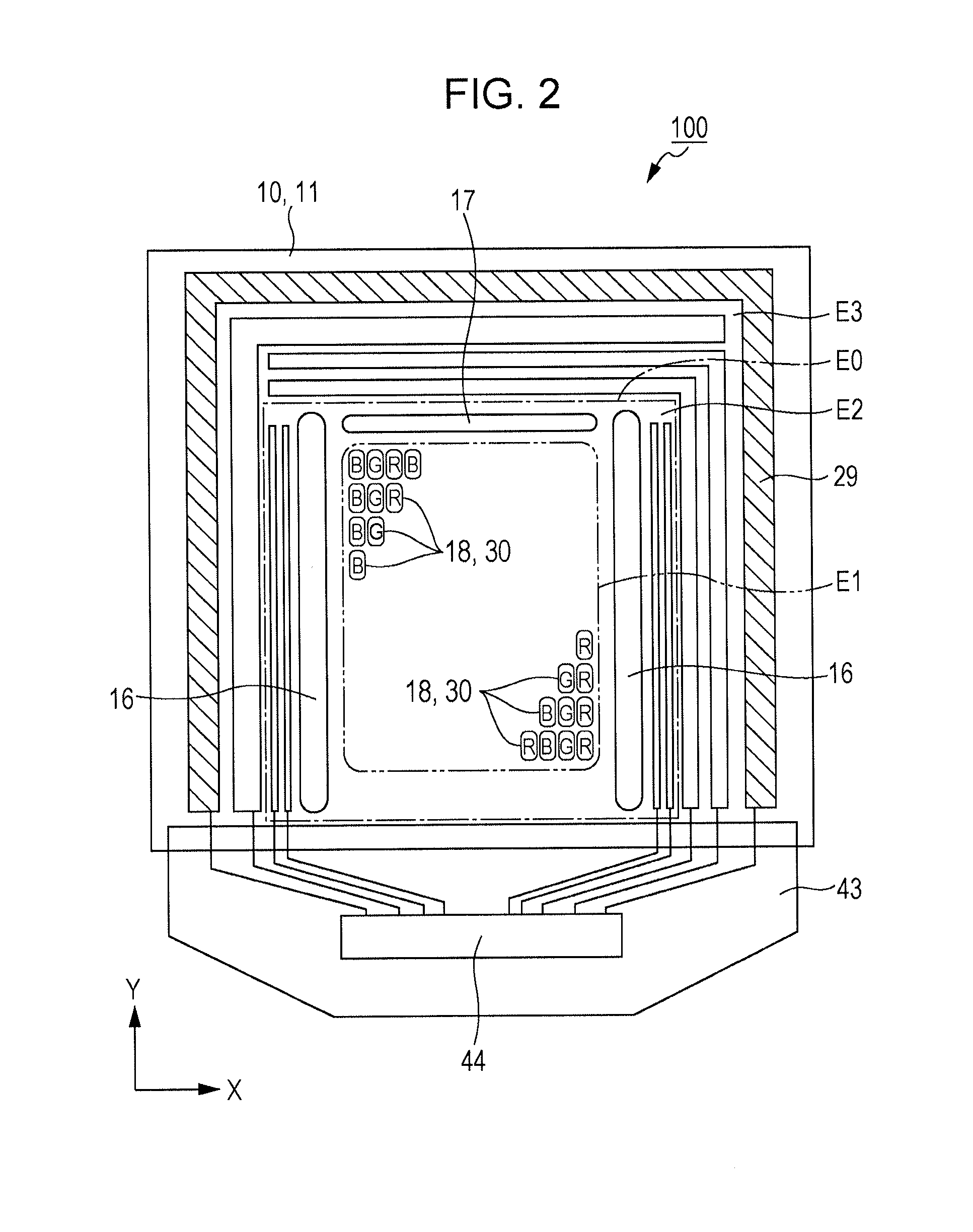
[0054]FIG. 1 is an equivalent circuit diagram illustrating an electrical configuration of the organic EL device of a first embodiment, FIG. 2 is a schematic plan diagram illustrating a configuration of the organic EL device of the first embodiment, FIG. 3 is a schematic plan diagram illustrating disposition of sub-pixels, and FIG. 4 is a schematic sectional-diagram illustrating a structure of sub-pixels taken along with a line IV-IV of FIG. 3.
[0055]As illustrated in FIG. 1, the organic EL device 100 of the present embodiment includes a plurality of scan lines 12 and a plurality of data lines 13 which are intersecting with one another, and a plurality of power supply lines 14 which is in parallel with the plurality of data lines 13, respectively. The organic EL device further includes a scan line driving circuit 16 where the plurality of scan lines 12 a...
second embodiment
Other Organic EL Device and Manufacturing Method Thereof
[0125]Next, an organic EL device of a second embodiment will be described referring to FIG. 10. FIG. 10 is a main portion schematic cross-sectional diagram illustrating a structure of sub-pixels of the organic EL device of the second embodiment. The organic EL device of the second embodiment causes a configuration of the convex portion 35 to be different from that of the organic EL device 100 of the first embodiment. Therefore, In the same configuration as the first embodiment, the same number is applied to omit detailed description. FIG. 10 corresponds to FIG. 4, and does not illustrate the driving transistor 23 and the like or the reflection layer 25 and the transparent layer 26 which configure the pixel circuit 20 on the base material 11 in the same manner as FIG. 4.
[0126]As illustrated in FIG. 10, the organic EL device 200 of the embodiment forms an element substrate 10 which has a base material 11, a plurality of organic E...
third embodiment
[0137]Next, an electronic equipment of the embodiment will be described referring to FIG. 12. FIG. 12 is a schematic diagram illustrating a head mounted display as the electronic equipment.
[0138]As illustrated in FIG. 12, a head mounted display (HMD) 1000 as an electronic equipment of the embodiment includes two display units 1001 provided corresponding to left and right eyes. By mounting the head mounted display 1000 on a head like glasses, a viewer M may see a letter or an image displayed on the display unit 1001. For example, when an image is displayed considering parallax on the left and right display units 1001, it is possible to see and enjoy a three-dimensional image.
[0139]In the display units 1001, the organic EL device 100 of the above described first embodiment (or the organic EL device 200 of the above described second embodiment) is mounted. Therefore, it is possible to have an excellent display quality and to provide a small and light head mounted di...
PUM
 Abstract
Description
Claims
Application Information