Methods and circuits for frequency modulation that reduce the spectral noise of switching regulators

Active Publication Date: 2005-11-03
ANALOG DEVICES INT UNLTD
View PDF2 Cites 57 Cited by
  • Summary
  • Abstract
  • Description
  • Claims
  • Application Information

AI Technical Summary

Benefits of technology

[0019] To provide greater flexibility to a user, the user may disable spread spectrum frequency operation and direct the oscillator to generate the

Problems solved by technology

A switching regulator introduces electromagnetic noise to an electronic application.
Although linear frequency modulation yields be

Method used


Image

  • Methods and circuits for frequency modulation that reduce the spectral noise of switching regulators
  • Methods and circuits for frequency modulation that reduce the spectral noise of switching regulators
  • Methods and circuits for frequency modulation that reduce the spectral noise of switching regulators

Examples


Example

[0075] In a first embodiment of frequency modulation circuit 18 of the present invention depicted in FIGS. 9 and 10, signal generator 20 comprises pseudo-random number generator 24 that supplies digital signals Q0−Qi having a uniform probability density distribution to digital-to-analog converter (“DAC”) 26. Pseudo-random number generator 24 comprises self-feeding shift register 28 having feedback circuit 30. Feedback circuit 30 may comprise logic that accept output signals from register 28 and generates a data signal derived therefrom. That data signal is fed back into the register's DATA_IN input. Although feedback circuit 30 is shown as accepting all signals output by register 28, one of ordinary skill in the art will recognize that feedback circuit 30 also may be configured to accept less signals. In general, only a few bits are needed. One of ordinary skill in the art will recognize that, rather than incorporating logic, feedback circuit 30 also may comprise a memory look-up ta...

Example

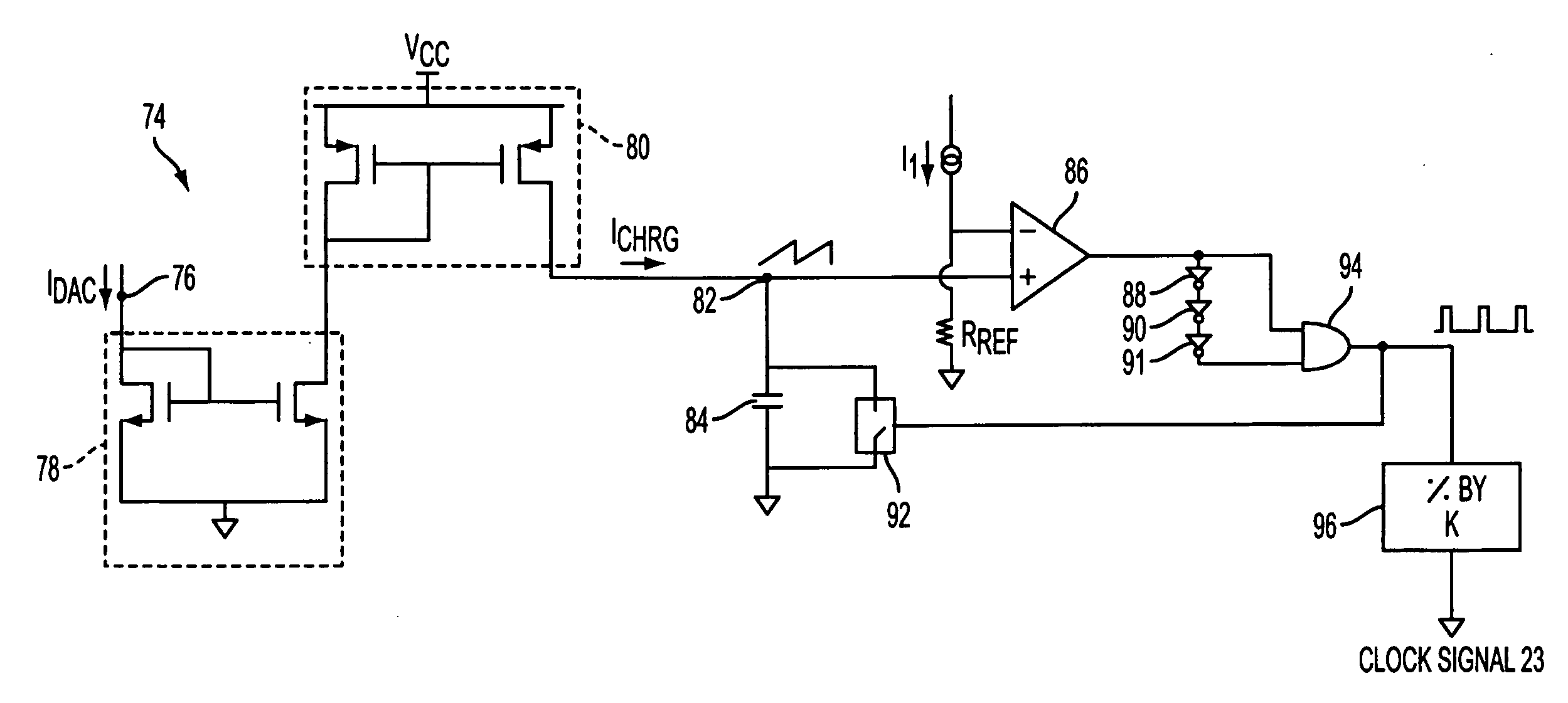
[0119] Referring now to FIG. 18, a third embodiment of oscillator 22 is described, in which the oscillator has a linear input-to-output transfer function. Oscillator 186 comprises a ring oscillator having timing capacitor 188 that is charged and discharged by a sourcing current source and a sinking current source (respectively) to generate a clock signal at output node 190. More specifically, to charge timing capacitor 188, oscillator 186 comprises a sourcing current source formed by diode-connected transistors 192 and 194 that respectively are coupled to mirroring transistors 196 and 198. The sourcing current source charges timing capacitor 188 with a current having a magnitude that is proportional to charging current ICHRG. The sinking current source of oscillator 186 is formed by diode-connected transistor 192 and mirroring transistor 200, which together discharge capacitor 188 with a current having a magnitude that is proportional to charging current ICHRG.

[0120] When the sourc...

Example

[0126] Referring now to FIG. 20, a fourth embodiment of oscillator 22 is described, wherein the oscillator has a linear input-to-output transfer function. In contrast to the current-controlled oscillators of FIGS. 13-15 and 18, the frequency of the clock signal generated by oscillator 220 is voltage-controlled. Oscillator 220 comprises amplifier 222 having a feedback loop and current mirror 224 that supplies as much current as needed to servo the inverting input of amplifier 222 at the voltage supplied to the non-inverting input. The servo current then is mirrored by current mirror 224 to generate a proportional current to charge timing capacitor 228. To discharge timing capacitor 228, oscillator 220 comprises comparator 227 that directs switch 229 to short circuit capacitor 228 to ground when it determines that the voltage across the capacitor has reached or exceeded constant reference voltage VREF.

[0127] The amount of current supplied to charge timing capacitor 228, and thus the ...


PUM


Abstract

The present invention comprises methods and circuits for spread spectrum frequency modulation that reduce peak spectral noise at the outputs or inputs of switching regulators. More specifically, the present invention modulates the operating frequency of the switching regulator in accordance with a frequency modulation waveform having a shape coordinated to a peak noise amplitude waveform that describes the correlation between the operating frequency of a switching regulator and the peak noise amplitude at the regulator's input or output absent spread spectrum frequency modulation.

Description

FIELD OF THE INVENTION [0001] The present invention relates to methods and circuits for spread spectrum frequency modulation that reduce the peak spectral noise of switching regulators. BACKGROUND OF THE INVENTION [0002] Switching regulators regulate voltage across a load connected to its output by varying the ON-OFF times of switching elements so that power is transmitted through the switching elements into energy storage elements. The energy storage elements then supply this power to the load. Switching regulators vary the ON-OFF times of the switching elements, in part, responsive to a clock signal generated by an oscillator. In a manner to be discussed in greater detail hereinbelow, the noise at the output of the switching regulator is dependent on the switching frequency of the clock signal, which hereinafter also will be referred to as the operating frequency of the switching regulator. [0003] A switching regulator introduces electromagnetic noise to an electronic application....

Claims


Application Information

Patent Timeline
IPC IPC(8): H02M3/00H03K3/84H03K5/156H03K7/06H04B15/02
CPCH02M1/44H02M3/156H04B2215/069H04B2215/067H04B15/04
Inventor CHEN, YUHUILAPORTE, DOUGFLATNESS, RANDY GUYDOBKIN, ROBERT C.
Owner ANALOG DEVICES INT UNLTD
Why Eureka
Try Eureka