Hermetically packaged MEMS G-switch

Inactive Publication Date: 2011-06-07
THE UNITED STATES OF AMERICA AS REPRESENTED BY THE SECRETARY OF THE NAVY
View PDF9 Cites 15 Cited by
  • Summary
  • Abstract
  • Description
  • Claims
  • Application Information

AI Technical Summary

Benefits of technology

[0007]A MEMS G-switch structure is provided having a bottom substrate layer, a top device layer and an intermediate oxide layer joining the bottom and top layers. At least one anchor portion is defined in the device layer. The device layer includes a mass moveable out of the plane of the device layer, and at least one spring arm having a first end connected to the mass and a second end connected to the anchor portion. The connection of the spring arm to the

Problems solved by technology

As these devices use folded springs to support the mass, the mass is also able to move in the plane of the substrate, which can lead to binding of the mass during spinning of the projectile.
In addition, the mass has a relatively large surface are

Method used


Image

  • Hermetically packaged MEMS G-switch
  • Hermetically packaged MEMS G-switch
  • Hermetically packaged MEMS G-switch

Examples


Example

[0019]The invention comprises a MEMS type acceleration switch. In some embodiments, the switch is non-latching. One of many exemplary applications for the invention is an impact detection sensor in a 25 mm ordnance round.

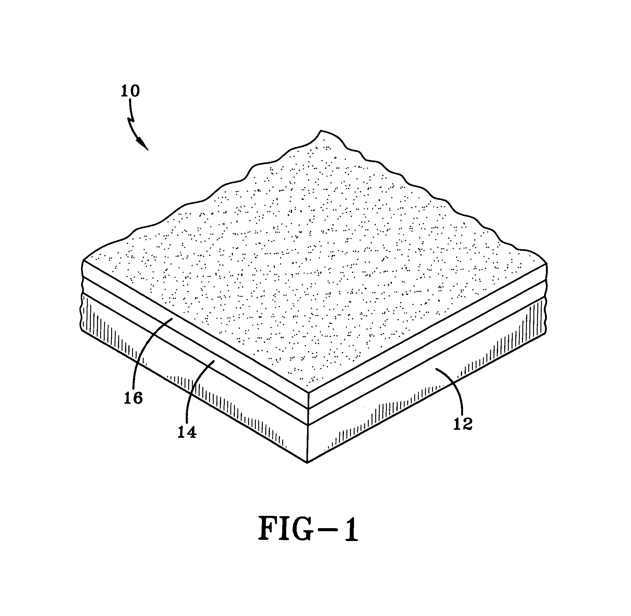
[0020]FIG. 1 illustrates a portion of an SOI (silicon on insulator) wafer 10 from which the switch of the present invention will be fabricated. The structure of FIG. 1 includes a silicon substrate 12 (also known as a bottom or handle layer) covered by an insulating layer 14, such as silicon dioxide, over which is deposited another silicon layer 16 (also known as the top or device layer), which is the layer from which the moveable parts of the switch will be fabricated.

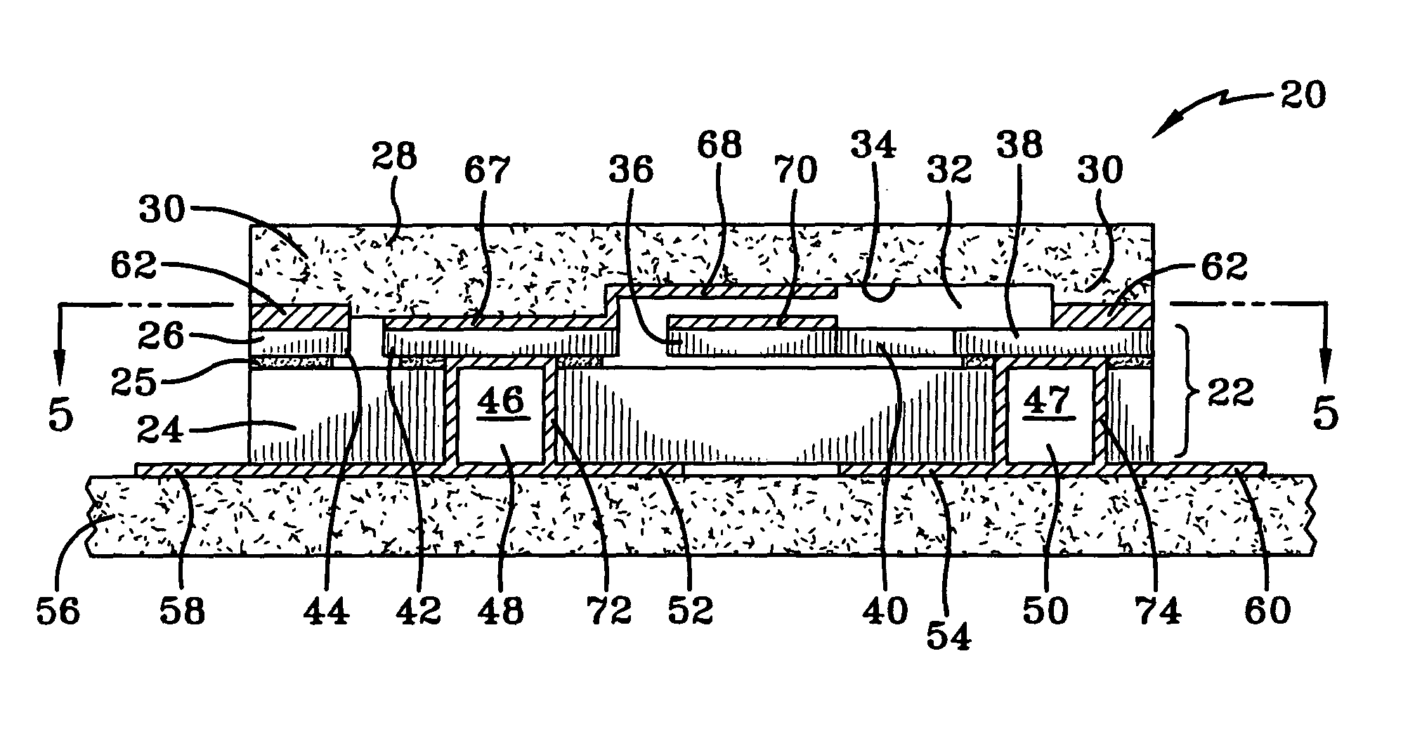
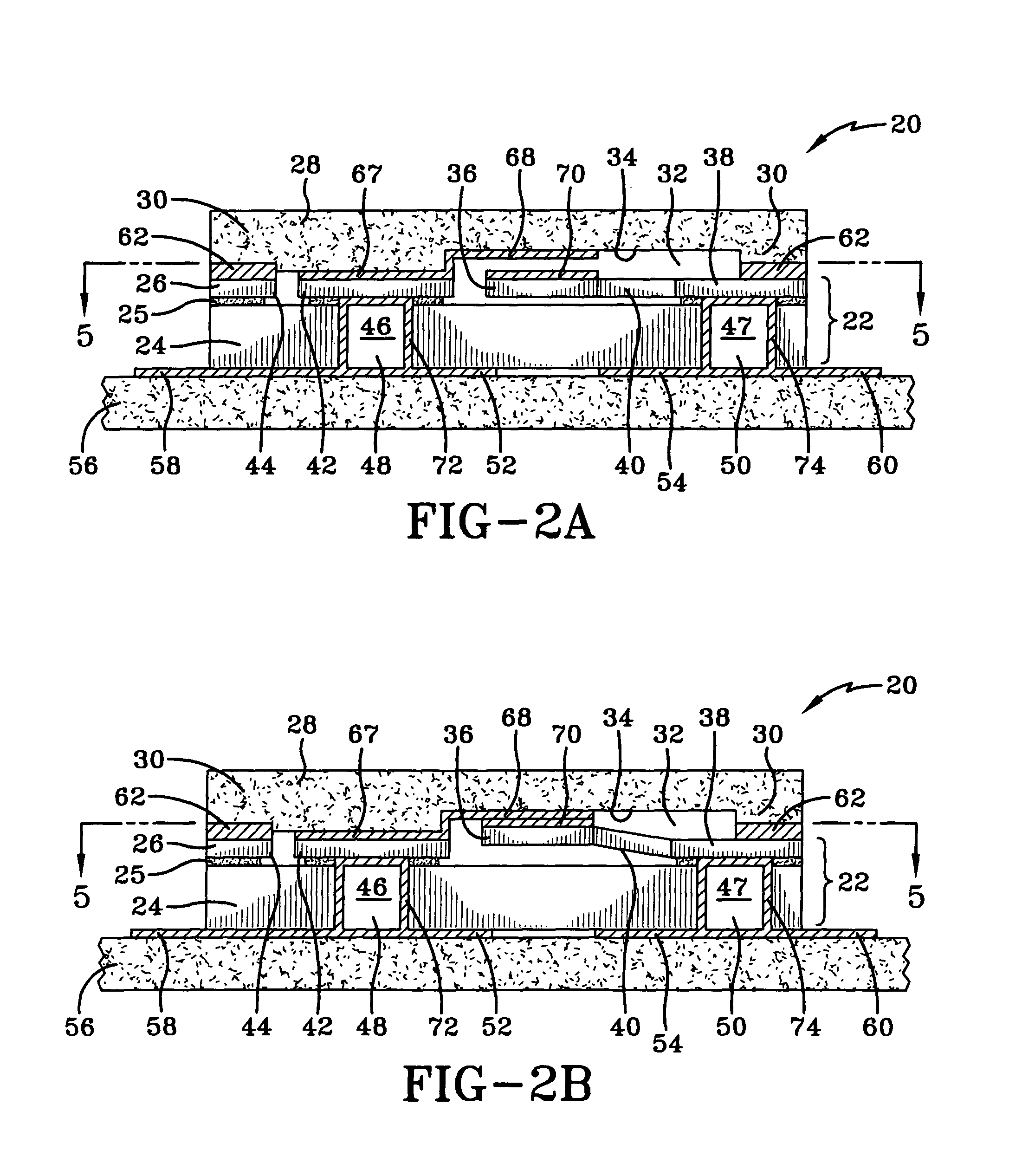
[0021]FIGS. 2A and 2B are sectional views of a G-switch 20 formed from a wafer similar to wafer 10 of FIG. 1, in respective open and closed positions. The switch 20 is fabricated from an SOI structure 22 having a substrate 24, an insulating layer 25 and a device layer 26. A cap wafer 28 is hermetically...


PUM


Abstract

A hermetically packaged G-switch includes a MEMS structure having a bottom substrate layer, a top device layer and an intermediate oxide layer. A mass disposed in the top device layer is connected to one, two or three anchor portions using spring arms. One end of a spring arm is connected to the mass and another end to an anchor portion. The connection to the anchor portion includes a T shaped arrangement, which has a torsional spring cross piece connected to the spring arm. A cap containing a conductive pad is hermetically sealed to the MEMS structure. When a predetermined acceleration is attained, the mass makes electrical contact with the conductive pad to close the G-switch.

Description

STATEMENT OF GOVERNMENT INTEREST[0001]The invention described herein may be manufactured and used by or for the Government of the United States of America for Governmental purposes without the payment of any royalties thereon or therefor.BACKGROUND OF THE INVENTION[0002]The invention relates in general to acceleration sensors and in particular to MEMS type acceleration sensors.[0003]Acceleration sensors and switches are used in various commercial and military applications, for example, projectiles that carry explosives. Acceleration sensors that close an electrical circuit upon impact of a projectile are often called impact sensors or G-switches (Gravity switches) or PD (point detonating) switches. Micro-electro mechanical systems (MEMS) are used in the fuzes and safe and arm systems of some projectiles. MEMS devices are small, lightweight, accurate, reliable and often cheaper than conventional devices. The MEMS G-switches shown in U.S. Pat. Nos. 6,737,979 and 6,619,123 move only in...

Claims


Application Information

Patent Timeline
IPC IPC(8): H01H35/02G01P15/135H01H35/14
CPCG01P1/023H01H35/14H01H1/0036G01P15/135G01P2015/0828
Inventor JEAN, DANIELCHEN, EZRA
Owner THE UNITED STATES OF AMERICA AS REPRESENTED BY THE SECRETARY OF THE NAVY
Why Eureka
Try Eureka