High quality thin dielectric layer and method of making same

a dielectric layer, high-quality technology, applied in the direction of semiconductor devices, basic electric elements, electrical equipment, etc., can solve the problems of poor quality of by-product oxide layers, low density of chemical oxide layers, and device thickness reduction to become comparabl

Active Publication Date: 2005-11-03
NXP USA INC
View PDF1 Cites 60 Cited by
  • Summary
  • Abstract
  • Description
  • Claims
  • Application Information

AI Technical Summary

Problems solved by technology

One such issue arises as semiconductor layers in such devices decrease in thickness to become comparable to the thickness of ubiquitous, but heretofore largely ignored, by-product oxide layers which are very thin but which are of poor quality.
These chemical oxide layers typically exhibit low density and poor quality relative to purposefully formed, thicker oxide layers of present and past generation semiconductor processes.

Method used


Image

  • High quality thin dielectric layer and method of making same
  • High quality thin dielectric layer and method of making same
  • High quality thin dielectric layer and method of making same

Examples


Embodiment Construction

)

[0011] The following discussion is intended to provide a detailed description of at least one example of the invention to help enable those skilled in the art to practice the invention. It is not intended to be limiting of the invention itself. Rather, any number of variations may fall within the scope of the invention which is properly defined in the claims following this description.

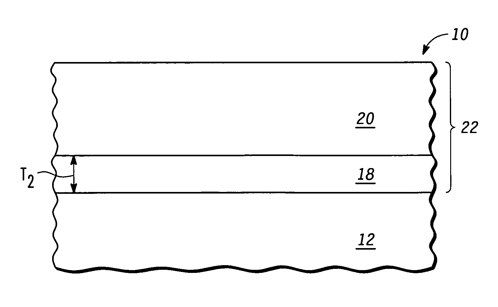
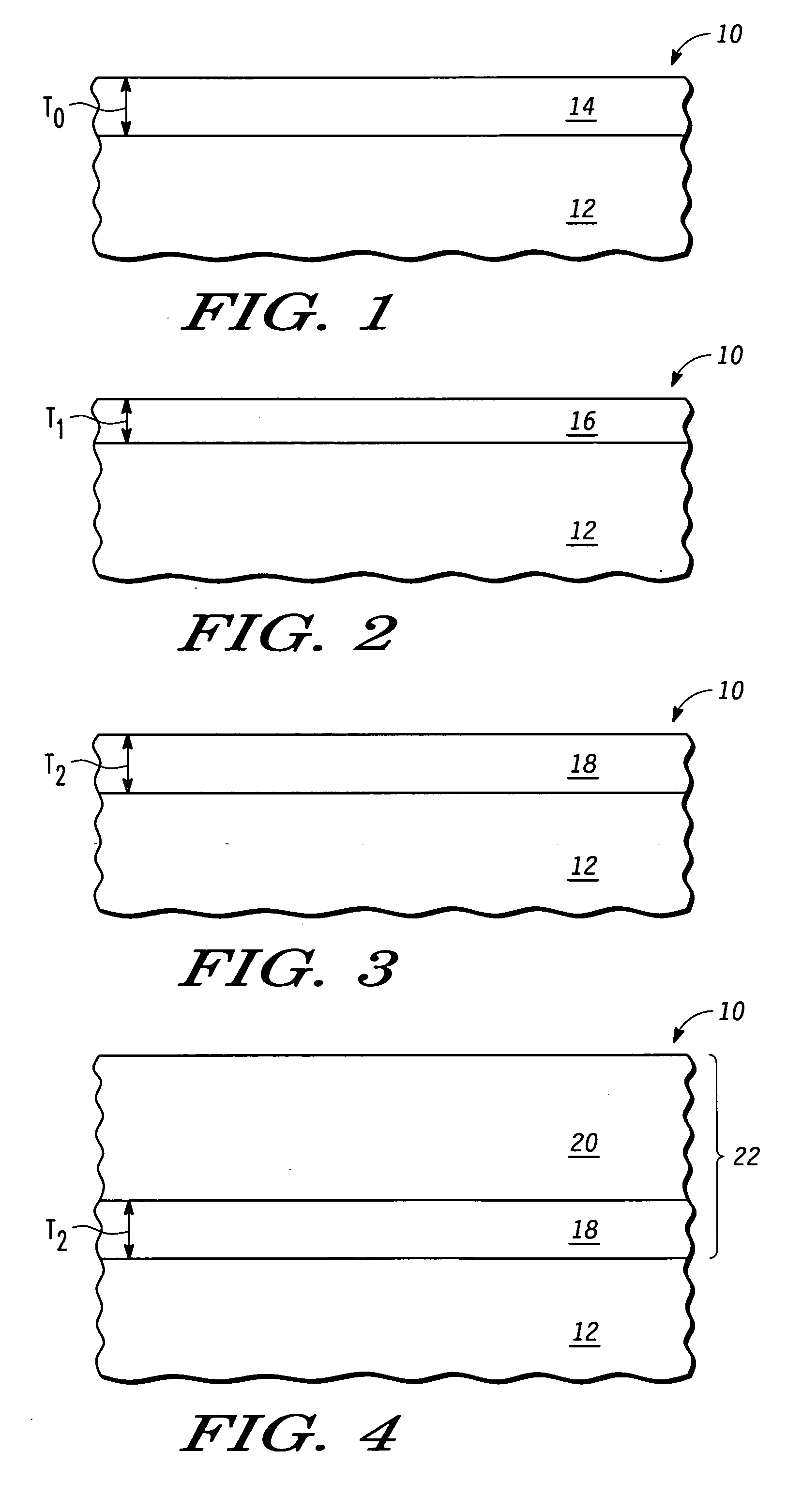
[0012]FIGS. 1-4 show cross-sectional views of a semiconductor wafer during stages in the manufacture of semiconductor devices (e.g., integrated circuits or specific devices therein) according to an embodiment of the present invention. As will be described in greater detail below, the illustrated embodiment provides a semiconductor device precursor with a substrate and base oxide layer (FIG. 1) and utilizes a high temperature double anneal process (FIGS. 2 and 3) to provide a thin (e.g., less than 13 angstroms) but high quality oxide layer (FIG. 3) as part of an overall integrated circuit device manuf...


PUM

PropertyMeasurementUnit
temperatureaaaaaaaaaa
time durationaaaaaaaaaa
temperatureaaaaaaaaaa

Abstract

A high quality thin dielectric layer is achieved by annealing a substrate and base oxide layer at a first temperature in a first ambient and subsequently annealing the substrate and base oxide layer at a second temperature in a second ambient, the base oxide layer overlying a top surface of the substrate. Prior to the first anneal, the base oxide layer has an initial thickness and density. The first anneal causes a first density and thickness change in the base oxide layer from the initial thickness and density to a first thickness and density, with no incorporation of a component of the ambient within the base oxide layer. The first thickness is less than the initial thickness and the first density is greater than the initial density. The second anneal causes a second density and thickness change in the base oxide layer from the first thickness and density to a second thickness and density. The second thickness is larger than the first thickness and the second density is on the order of the greater than or equal to the first density.

Description

BACKGROUND [0001] 1. Field [0002] The present invention relates to semiconductor device manufacturing, and, more particularly, to apparatus and methods related to making high quality, thin dielectric layers. [0003] 2. Description of the Related Art [0004] As semiconductor manufacturing process dimensions scale downward to provide increasingly smaller semiconductor devices, many previously minor issues gradually become important enough to warrant attention by the industry. One such issue arises as semiconductor layers in such devices decrease in thickness to become comparable to the thickness of ubiquitous, but heretofore largely ignored, by-product oxide layers which are very thin but which are of poor quality. [0005] For example, the well known RCA cleaning process (so named for its corporate developer, the Radio Corporation of America) often leaves behind a chemical oxide layer. These chemical oxide layers typically exhibit low density and poor quality relative to purposefully for...

Claims


Application Information

Patent Timeline
Patent Type & Authority Applications(United States)
IPC IPC(8): H01L21/28H01L21/314H01L21/316H01L21/8238H01L29/51
CPCH01L21/28185H01L21/28194H01L21/28202H01L29/513H01L21/3141H01L21/31645H01L21/28211H01L21/02299H01L21/02255
Inventor LUO, TIEN-YINGADETUTU, OLUBUNMI O.TSENG, HSING-HUANG
Owner NXP USA INC
Why Eureka
Try Eureka