Organic electro luminescence device and fabrication method thereof

a luminescence device and organic technology, applied in the direction of electroluminescent light sources, organic semiconductor devices, thermoelectric devices, etc., can solve the problems of light weight and slimming, difficult to secure a sufficient aperture ratio for a small-sized display device, and non-luminous display devices. achieve the effect of simple and stable operation

Active Publication Date: 2005-11-10
LG DISPLAY CO LTD
View PDF11 Cites 42 Cited by
  • Summary
  • Abstract
  • Description
  • Claims
  • Application Information

AI Technical Summary

Benefits of technology

[0028] An OELD and a fabrication method thereof enabling its simple and stable operation are provided in which an array element and an organic electro luminescent diode are formed in different substrates, a driving TFT for driving each pixel is a p-Si TFT, a first electrode (anode) of the organic electro luminescent diode is connected to a drain electrode of the driving TFT, and a transparent second electrode (cathode) is unnecessary.

Problems solved by technology

However, the LCD is a non-luminous display device and has technical limitations in brightness, contrast, viewing angle, and screen size.
Also, since the OELD does not require a backlight assembly, it is lightweight and slim.
For this reason, it is difficult to secure a sufficient aperture ratio for a small-sized display device.
The entire process yield is greatly restricted by the latter process, that is, the process of forming the organic electro luminescent diode.
For example, even though excellent array elements are formed, if foreign particles or other factors cause defects in forming the organic electro luminescent layer using a thin film of about 1000 Å thick, the corresponding OELD is defective.
Accordingly, expense and material cost spent in fabricating the non-defective array element occurs, resulting in the reduction of the yield.

Method used


Image

  • Organic electro luminescence device and fabrication method thereof
  • Organic electro luminescence device and fabrication method thereof
  • Organic electro luminescence device and fabrication method thereof

Examples


Embodiment Construction

[0041] Reference will now be made in detail to the preferred embodiments of the present invention, examples of which are illustrated in the accompanying drawings. Wherever possible, the same reference numbers will be used throughout the drawings to refer to the same or like parts.

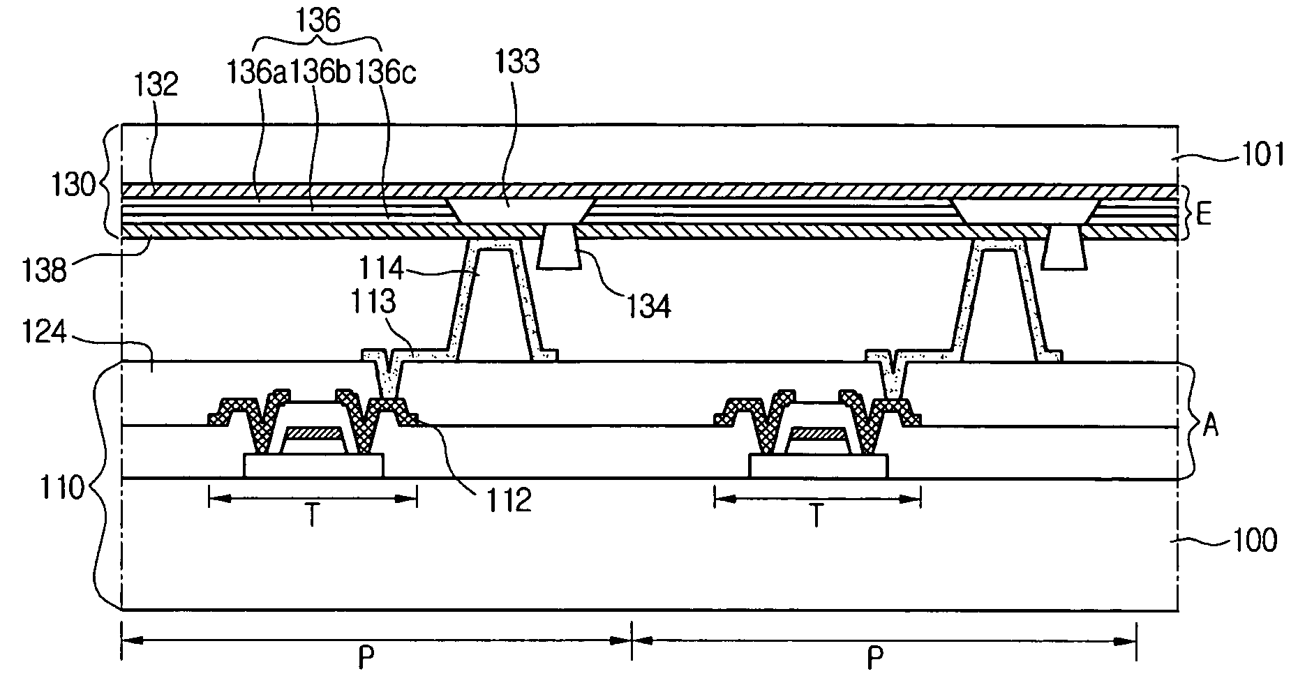
[0042] Before describing the present invention, reference will be made to a dual panel type OELD. FIG. 4 is a schematic sectional view of a dual panel type OELD. For simplicity in description, only two neighboring sub-pixel regions are illustrated in FIG. 4.

[0043] Referring to FIG. 4, first and second substrates 110 and 130 are arranged spaced apart from each other by a predetermined interval. An array element A is formed on an upper surface of a transparent substrate 100 of the first substrate 110, and an organic electro luminescent diode E is formed on a lower surface of a transparent substrate 101 of the second substrate 130. Edge portions of the first and second substrates 110 and 130 are encapsulated...


PUM


Abstract

An organic electro luminescence device is provided. In the organic electro luminescence device, first and second electrodes are arranged to face each other and to be spaced apart from each other by a predetermined interval, and includes sub-pixels for reproducing an image. An array element is formed in the first substrate per sub-pixel, and includes at least one TFT. An organic electro luminescent diode is formed in the second substrate per sub-pixel. A spacer covered with a metal portion for electrically connecting the first and second substrates. A drain electrode of the TFT and a first electrode (anode) of the organic electro luminescent diode are electrically connected by the spacer covered with the metal portion.

Description

PRIORITY CLAIM [0001] This application claims the benefit of Korean Patent Application No. P2004-32578 filed on May 10, 2004, which is hereby incorporated by reference. FIELD OF THE INVENTION [0002] The present invention relates to an organic electro luminescence device and a fabrication method thereof, and more particularly, to an organic electro luminescence device using a poly-silicon (p-Si) TFT as a driving element and a fabrication method thereof. DESCRIPTION OF THE RELATED ART [0003] In the fields of flat panel display devices, a liquid crystal display device (LCD) is widely used because it is lightweight and has low power consumption. However, the LCD is a non-luminous display device and has technical limitations in brightness, contrast, viewing angle, and screen size. Therefore, new flat panel display devices capable of overcoming these drawbacks have been developed actively. [0004] One of the new flat panel display devices is an organic electro luminescence device (OELD). S...

Claims


Application Information

Patent Timeline
Patent Type & Authority Applications(United States)
IPC IPC(8): H01L21/77H01L21/84H05B33/04H01L27/12H01L27/15H01L27/32H01L31/036H01L51/40H01L51/50H05B33/06H05B33/10H05B33/12H05B33/14H05B33/26H05B44/00
CPCH01L27/3246H01L2251/5315H01L27/3253H10K59/1275H10K59/122H10K2102/3026H10K59/10H05B33/26
Inventor BAE, SUNG JOONLEE, JAE YOON
Owner LG DISPLAY CO LTD
Why Eureka
Try Eureka