Method of defect inspection

a defect inspection and defect technology, applied in the direction of measurement devices, semiconductor/solid-state device testing/measurement, instruments, etc., can solve the problems of reducing the performance of integrated circuits, forming defects, and tiny particles, so as to avoid redundant inspection efforts, reduce the cost of bare wafers, and respond quickly

Active Publication Date: 2005-11-10
POWERCHIP SEMICON MFG CORP
View PDF14 Cites 10 Cited by
  • Summary
  • Abstract
  • Description
  • Claims
  • Application Information

AI Technical Summary

Benefits of technology

[0035] It is an advantage of the present invention against the prior art that the daily check in the prior art is integrated into the in-line defect inspection process, enabling operators to quickly respond to any abnormality of either the processes or the tools. In addition, by eliminating the manual inspection procedures in the prior art, not only the consumption of monitor wafers with high material cost is reduced, but inadequate operation of the tools by the operators frequently caused by the switches between manual and automatic operating modes is also prevented. Moreover, the defect inspection method in the present invention avoids redundant inspection efforts towards the wafers under production. Consequently, the manufacturing efficiency is increased as well.
[0036] These and other objectives of the present invention will no doubt become obvious to those of ordinary skill in the art after reading the following detailed description of the preferred embodiment that is illustrated in the various figures and drawings.

Problems solved by technology

In the semiconductor manufacturing, some tiny particles and defects, which frequently reduce the performance of integrated circuits, are sometimes formed during various processes unavoidably.
However, the cost of bare wafer, especially a 12″ wafer, is so high that the production cost would be severely increased if we use it for daily check.
In addition, many integrated defects occur only after a series of processes and therefore can not be found on a bare wafer.
As a result, the daily check procedure turns out to be ineffective.
Moreover, the production tool, such as tool 20a, cannot simultaneously be inspected by the daily check procedure in FIG. 2 and perform manufacturing processes on product wafers.
Therefore, in order to maintain the utilization of tool capacity at a certain level, the daily check procedure is rarely daily performed, leading to a inefficient monitor of the tool.
As a result, some tools may not be installed with any sampling cassette and therefore are not inspected.
However, the chosen cassettes sometimes do not contain the defect information about previous processes since they are not necessarily sampling cassettes.
The yield rate may be lowered due to inadequate judgment of operator towards the inspected tool caused by the improper operation of the SEM.
Moreover, the methods in FIG. 3 and FIG. 4 are performed by utilizing product wafers, which frequently leads to redundant inspection efforts.
As a result, the production lead-time and labor cost are both increased.

Method used


Image

  • Method of defect inspection
  • Method of defect inspection
  • Method of defect inspection

Examples


Embodiment Construction

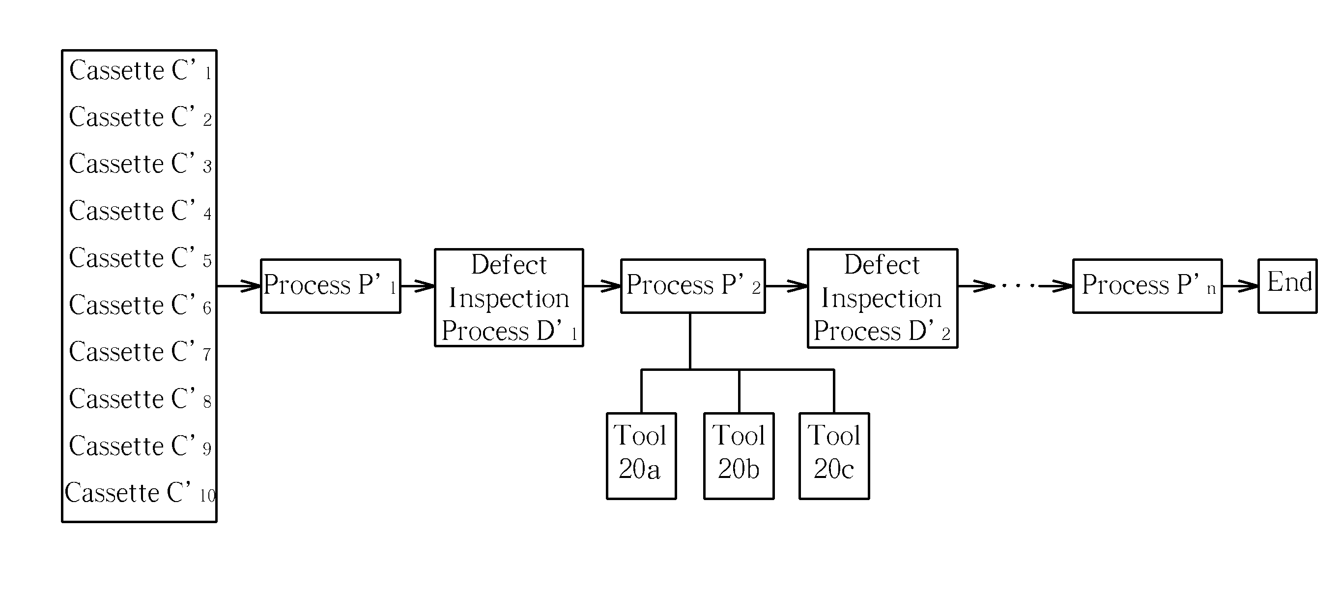
[0048] Please refer to FIG. 5, which is a flow chart of semiconductor manufacturing according to the present invention. As shown in FIG. 5, a plurality of cassettes, cassettes C′1 to C′10 for instance, is provided, and each of the cassettes C′1 to C′10 comprises 25 wafers, wafers W1 to W25. Then the information of cassettes is C′1 to C′10 input into a process control server (not shown) by a process engineer, and several cassettes and wafers are selected as sampling cassettes and sampling wafers, respectively. For example, the cassettes C′3, C′5, C′6 and C′10 are selected to be the sampling cassettes, and the wafers W1, W10, W20 and W24 in each of the sampling cassettes are selected to be the sampling wafers. A plurality of processes P′1 to P′n are performed on the cassettes C′1 to C′10 thereafter according to an automatic manufacturing schedule installed in the process control server, so as to form various devices on each of the wafers in the cassettes C′1 to C′10, such as metal-oxi...


PUM

PropertyMeasurementUnit
defect inspectionaaaaaaaaaa
defectaaaaaaaaaa
numbers of defectsaaaaaaaaaa

Abstract

A plurality of cassettes, each having a plurality of wafers respectively having a first defect information, is selected. Each of the cassettes is then assigned to a corresponding tool having at least one reaction chamber, and the wafers are substantially equally assigned to the reaction chambers. A first process is then performed on each of the wafers in the reaction chamber. Finally, a first defect inspection process is performed on each of the wafers.

Description

BACKGROUND OF INVENTION [0001] 1. Field of the Invention [0002] The present invention relates to a method of defect inspection, and more specifically, to an in-line defect inspection method for daily check. [0003] 2. Description of the Prior Art [0004] In the semiconductor manufacturing, some tiny particles and defects, which frequently reduce the performance of integrated circuits, are sometimes formed during various processes unavoidably. Therefore, different inspections are performed on semiconductor devices during the production in order to adjust production parameters, ensuring the reliability and yield of manufacturing processes by preventing the appearances of defects. [0005] Please refer to FIG. 1, which represents a flow chart of semiconductor manufacturing according to the prior art. As shown in FIG. 1, a plurality of cassettes, C1, C2 . . . to C10, is provided, and each of the cassettes C1 to C10 comprises a plurality of wafers. Then the data of cassettes C1 to C10 is rec...

Claims


Application Information

Patent Timeline
Patent Type & Authority Applications(United States)
IPC IPC(8): G01N21/00H01L21/00H01L21/66
CPCH01L21/67276H01L21/67253
Inventor LIN, LONG-HUICHEN, CHIA-YUN
Owner POWERCHIP SEMICON MFG CORP
Why Eureka
Try Eureka