Integrated strain gages for board strain characterization

a technology of strain characterization and integrated strain gages, which is applied in the direction of instruments, force/torque/work measurement apparatus, instruments, etc., can solve the problems of mechanical strain, assembly may become damaged, pcb to expand,

Active Publication Date: 2005-11-17
ORACLE INT CORP
View PDF7 Cites 26 Cited by
  • Summary
  • Abstract
  • Description
  • Claims
  • Application Information

AI Technical Summary

Benefits of technology

[0009] A printed circuit board (PCB) having an integrated strain gage is disclosed. In one embodiment, a PCB includes a component footprint suitable for mounting an electronic component. A

Problems solved by technology

Some processes, such as a wave solder operation or an IR (infrared) reflow operation may strain a PCB thermally and thus cause the PCB to expand.
Other manual handling processes may also result in mechanical strain.
If these limits are exceeded, the assembly may become damaged.
Signal lines can also be damaged if the strain exceeds limits.
However, the locations of these strain gages, while close to the BGA footprint, are not ideal.
Various factors, such as the thermal characteristics o

Method used


Image

  • Integrated strain gages for board strain characterization
  • Integrated strain gages for board strain characterization
  • Integrated strain gages for board strain characterization

Examples


Embodiment Construction

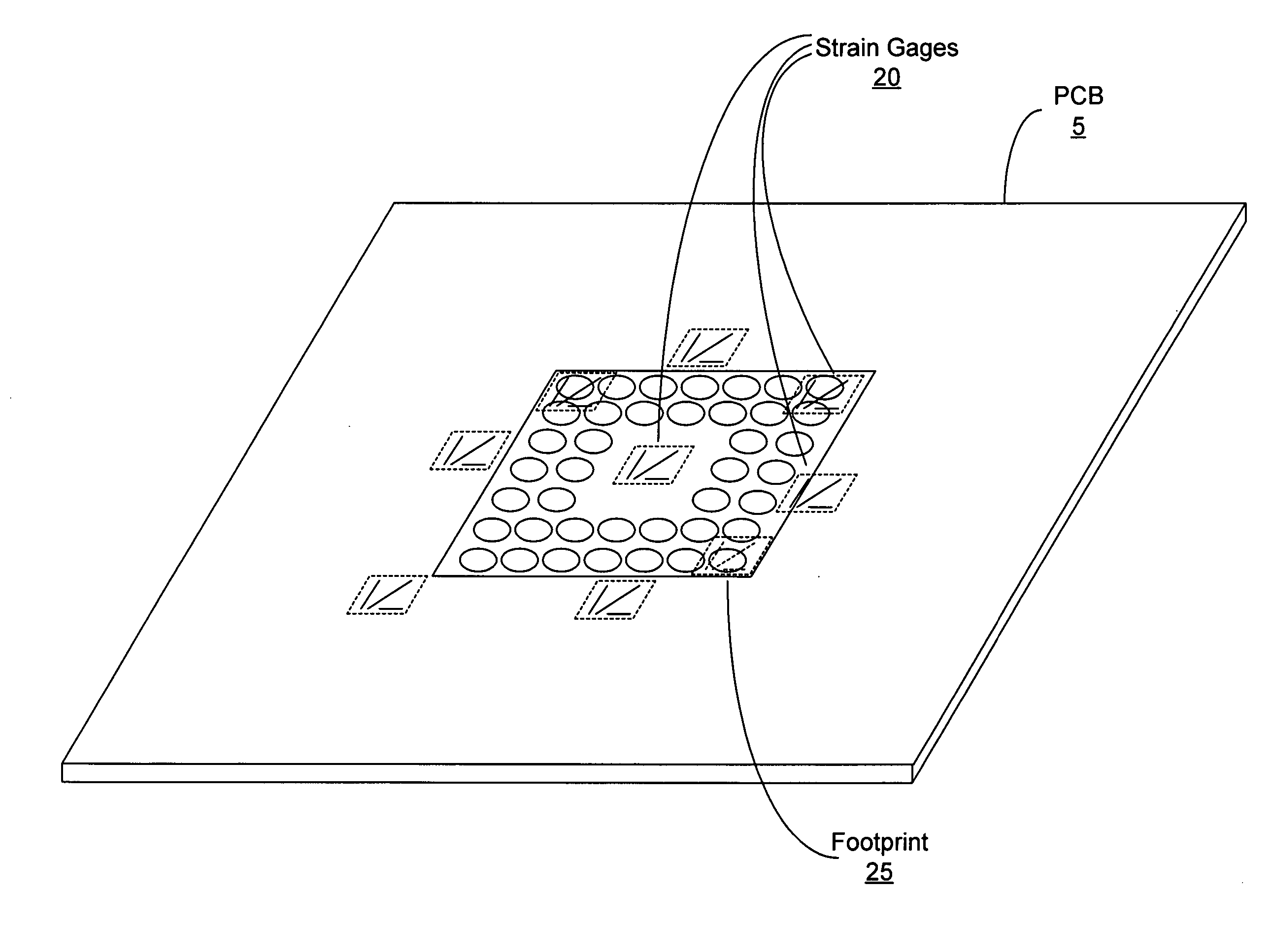
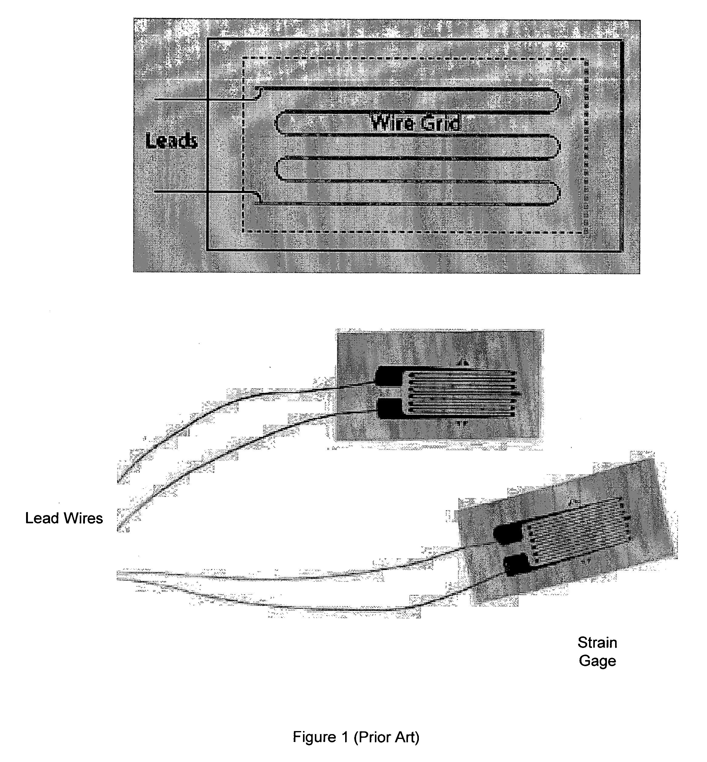
[0020] Turning now to FIG. 3, a drawing of one embodiment of a PCB having integrated strain gages is shown. In the embodiment shown, three different strain gages 20 (denoted by dashed lines) are located primarily within an internal layer of PCB 5. Strain gages 20 may each include a conductor configuration of any one of many commonly available strain gages, including the strain gages shown in FIG. 1.

[0021] Strain gages 20 are located within the layers of PCB 5 in the vicinity of footprint 25. One of the strain gages 20 is located under footprint 25 in its entirety. Another one of strain gages 20 is located partially under footprint 25. A third strain gage 20 is located in the vicinity of footprint 25, although no part of this strain gage is actually under footprint 25. The actual locations of strain gages 20 in various embodiments may be determined in part by considerations such as signal routing density or other constraints.

[0022] Footprint 25 is a footprint suitable for mounting ...


PUM


Abstract

A printed circuit board (PCB) having an integrated strain gage. In one embodiment, a PCB includes a component footprint suitable for mounting an electronic component. A strain gage is integrated into the PCB in a location under the component footprint. The strain gage includes at least one electrical conductor that is accessible for resistance measurements.

Description

BACKGROUND OF THE INVENTION [0001] 1. Field of the Invention [0002] This invention relates to printed circuit boards, and more particularly, a method and apparatus for measuring mechanical strain in a printed circuit board. [0003] 2. Description of the Related Art [0004] During the manufacturing of electronic assemblies including printed circuit boards (PCB's), various processes may introduce mechanical strains. Some processes, such as a wave solder operation or an IR (infrared) reflow operation may strain a PCB thermally and thus cause the PCB to expand. Other processes such as in-circuit test (ICT) may strain the PCB mechanically, as an ICT often times requires the assembly to be secured in a caged fixture that is operated by a vacuum. Other manual handling processes may also result in mechanical strain. [0005] The mechanical strain placed on a PCB during the manufacturing process of an electronic assembly must be kept within certain limits. If these limits are exceeded, the assem...

Claims


Application Information

Patent Timeline
IPC IPC(8): G01L1/00G01L1/22G01L5/00H05K1/02H05K1/11H05K1/16
CPCG01L5/0047H05K1/0268H05K1/0271H05K1/111Y10T117/1044H05K2201/10151H05K2201/10734H05K2203/163H05K1/16G01L1/22
Inventor ONG, BRETT C.NEWMAN, KEITH G.
Owner ORACLE INT CORP
Why Eureka
Try Eureka