Semiconductor memory component in cross-point architecture

a technology of memory components and semiconductors, applied in semiconductor devices, digital storage, instruments, etc., can solve the problems of increasing the surface area taken up by each memory cell, affecting the performance of the memory cell, so as to increase the conductivity of the memory cell

Inactive Publication Date: 2005-11-17
ADESTO TECH
View PDF4 Cites 40 Cited by
  • Summary
  • Abstract
  • Description
  • Claims
  • Application Information

AI Technical Summary

Benefits of technology

[0014] In this memory cell arrangement in cross-point architecture, the programmable metalization memory cells are provided with integrated select diodes that are formed by a pn junction that is present between a chalcogenide glass, in particular arsenic sulfide, germanium sulfide, arsenic selenide or germanium selenide, and an n-conductively doped bit line. On that side of the chalcogenide glass that is remote from the bit line there is an electrode, which may in particular be a si

Problems solved by technology

On the other hand, what are known as disturb effects occur with a cross-point architecture, caused by the fact that during the write, erase and read operations voltages are also present at the memory cells, which have not been selected.
Nevertheless, during the read operation, for example, the unselected

Method used


Image

  • Semiconductor memory component in cross-point architecture
  • Semiconductor memory component in cross-point architecture
  • Semiconductor memory component in cross-point architecture

Examples


Embodiment Construction

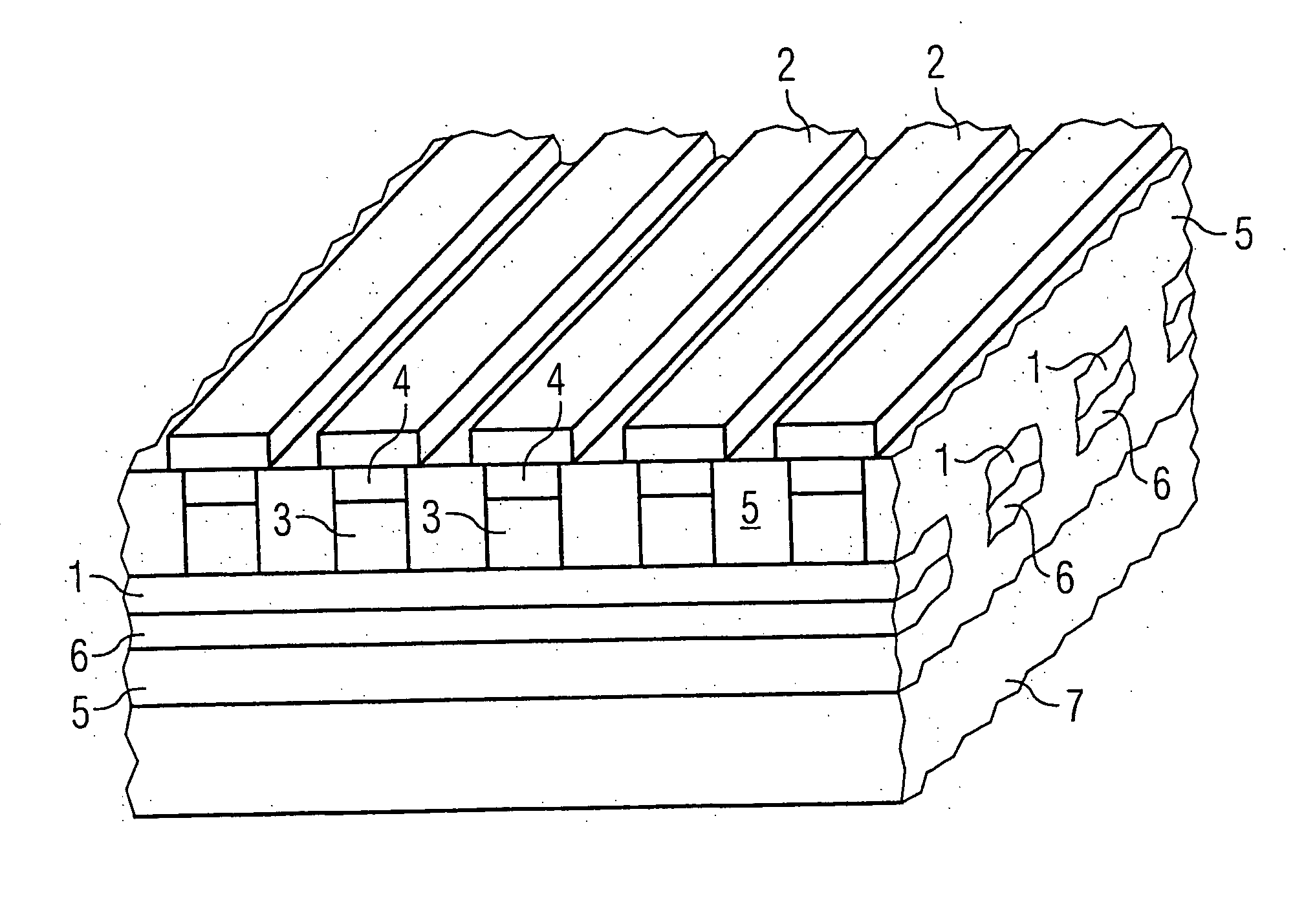
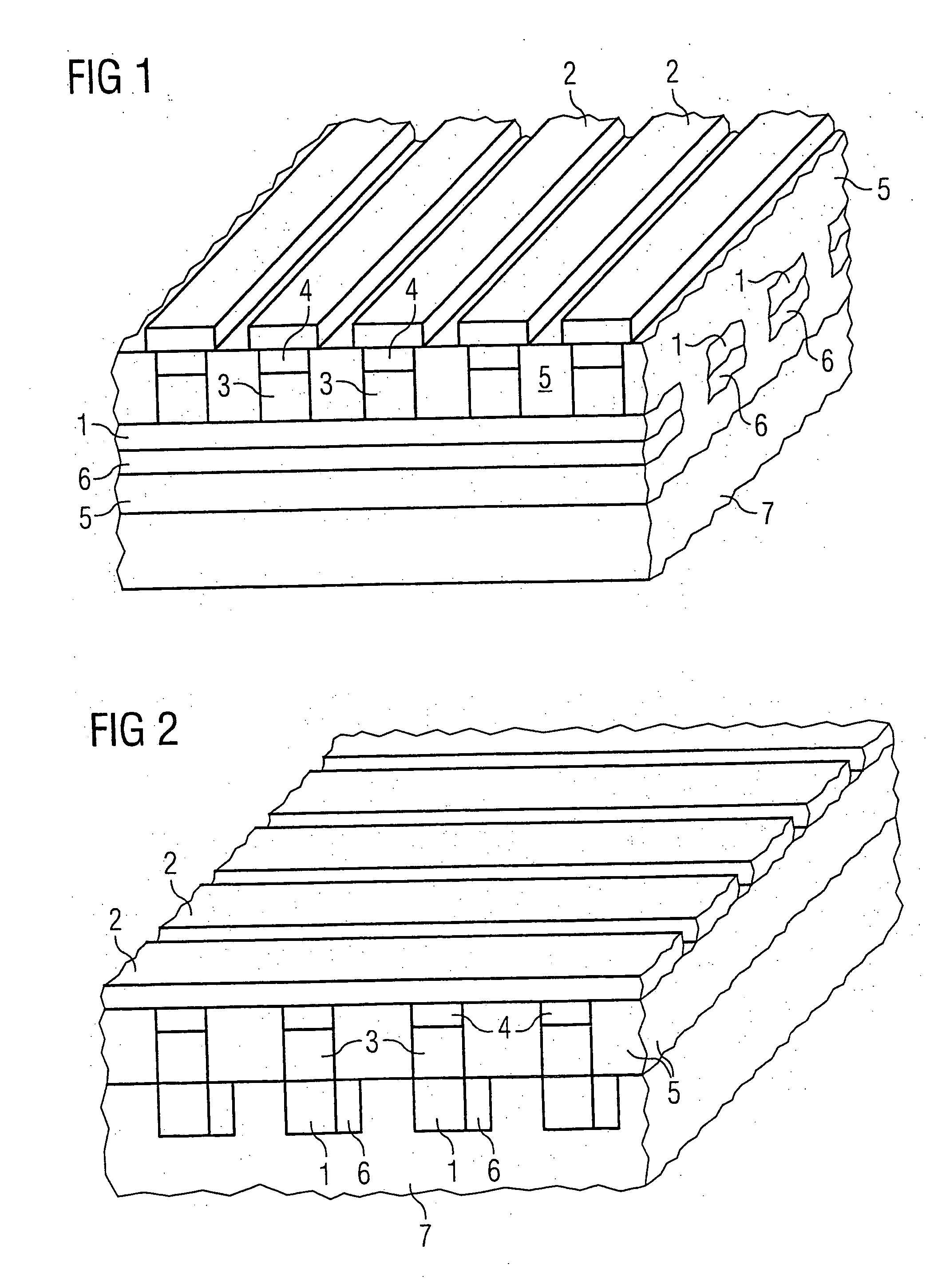
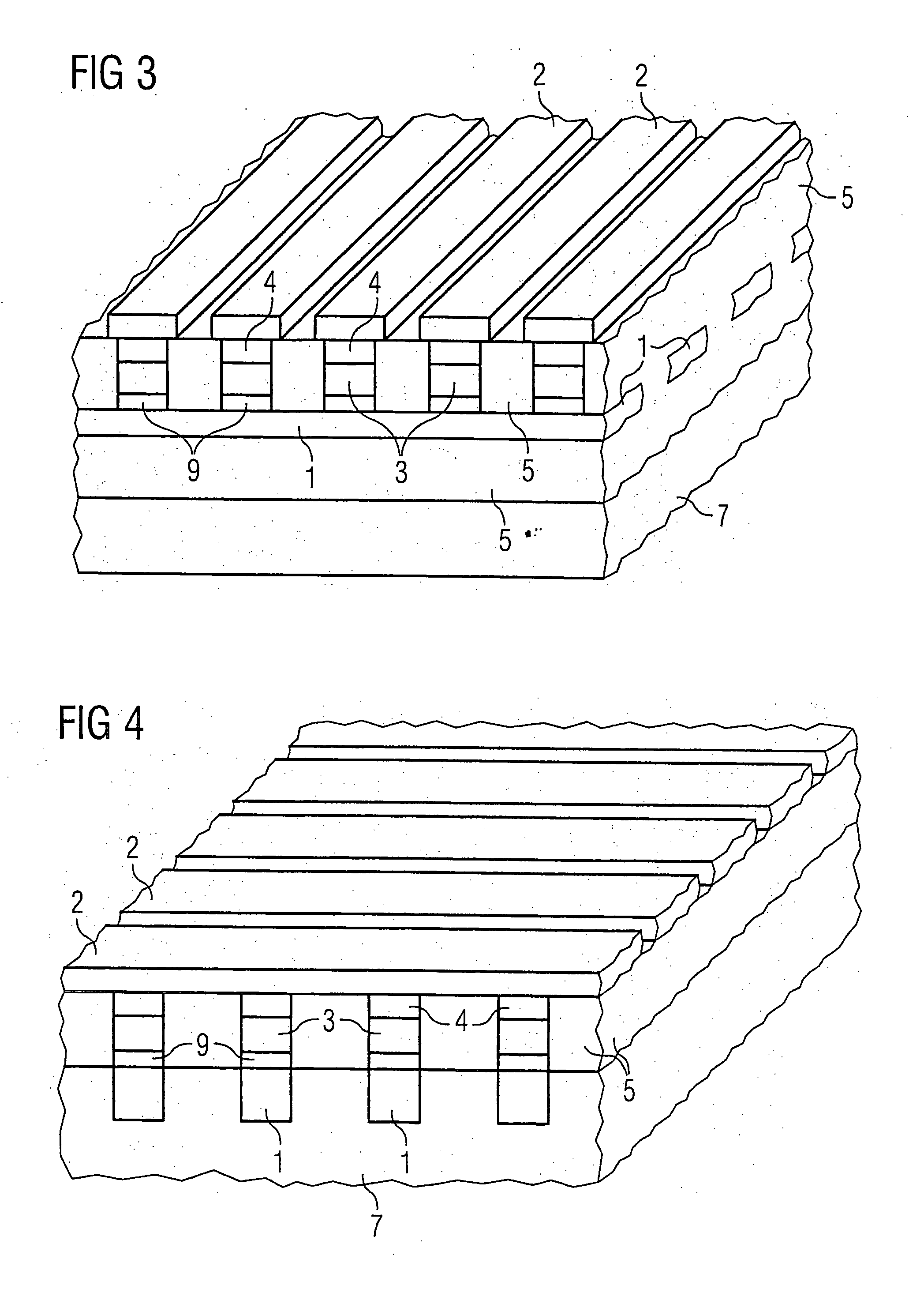
[0023]FIG. 1 illustrates a sectional view of a preferred configuration of a semiconductor memory component. The bit lines 1 are arranged parallel to and at a distance from one another below the memory cells, while the word lines 2 are arranged on the top side, running parallel to and at a distance from one another and transversely with respect to the bit lines. The word lines 2 may be a material that is used for interconnect structures, e.g., Al, Cu or W. At a respective crossing point of a corresponding bit line 1 and a word line 2 there is a programmable metalization memory cell, which comprises a storage region 3 and an electrode 4.

[0024] The storage region 3 contains a chalcogenide glass that, in combination with the topside electrode 4, forms a programmable metalization memory cell. The chalcogenide glass is undoped and therefore p-conducting at least adjacent to the bit line 1. The bit line is n-doped semiconductor material, e.g., n+-doped polysilicon, so that there is a pn j...


PUM


Abstract

A programmable metallization memory cell with a storage region (3) formed from a chalcogenide glass and an electrode (4) which is preferably silver is located at the crossing point of a respective bit line (1) and a respective word line (2). There is a pn junction between the bit lines (1) and the chalcogenide glass.

Description

[0001] This application claims priority to German Patent Application 102004020575.2, which was filed Apr. 27, 2004 and is incorporated herein by reference. TECHNICAL FIELD [0002] The present invention relates generally to semiconductor devices, and more particularly to a semiconductor memory component in cross-point architecture. BACKGROUND [0003] In semiconductor memory components in cross-point architecture, the memory cells are arranged at the crossing points of the bit lines and word lines. The bit lines are in each case arranged parallel to and at a distance from one another, and the word lines, transversely with respect to the bit lines, are likewise arranged parallel to and at a distance from one another. Each bit line crosses each word line at a location at which a respective memory cell is arranged. Resistively switching storage media are generally used for this type of architecture. The memory cell is selected by addressing the bit line and the word line which lead to the ...

Claims


Application Information

Patent Timeline
IPC IPC(8): G11C11/00G11C13/02G11C16/02H01L27/24
CPCG11C13/0011G11C2213/72H01L27/2409H01L27/2463H01L45/085H01L45/1233H01L45/1683H01L45/1266H01L45/141H01L45/142H01L45/143H01L45/1641H01L45/1253H10B63/20H10B63/80H10N70/245H10N70/826H10N70/841H10N70/8416H10N70/8822H10N70/882H10N70/8825H10N70/041H10N70/066
Inventor HAPP, THOMAS D.SYMANCZYK, RALF
Owner ADESTO TECH
Why Eureka
Try Eureka